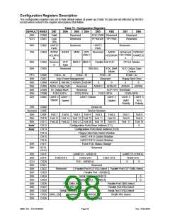
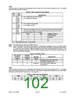
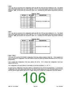
CR05
CR05 can only be accessed in the configuration state and after the CSR has been initialized to 05H. The default
value after power up is 00H (Table 82).
Table 82 - CR05: Floppy Disk Setup Register
BIT
BIT
NO.
NAME
DESCRIPTION
0 = FDC Outputs are open drain (default).
1 = FDC Outputs are push-pull.
01
FDC
Output
Type
Control
(R/W)
11,2 FDC
0 = FDC Outputs Active (default).
1 = FDC Outputs Tri-State.
Output
Control
(R/W)
2
FDC
DMA
Mode
0 = Burst mode is enabled for the FDC FIFO execution phase data transfers (default).
1 = Non-Burst mode enabled. The FDRQ and FIRQ pins are strobed once for each
byte transferred while the FIFO is enabled.
4,3 DenSel
BIT 4
BIT 3
DENSEL OUTPUT
0
0
1
1
0
1
0
1
Normal (default)
Reserved
1
0
5-7 Reserved Read Only. A read returns 0.
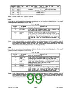
Note1: Bits CR05[1:0] do not affect the Parallel Port FDC.
Note2: In the FDC37N3869, the behavior of the DRVDEN1 Control CR03.4 depends upon the FDC Output Control
CR05.1 (Table 82). If the FDC Output Control is active DRVDEN1 will behave as described in the 669FR;
i.e., if CR03.4 is 0 the DRVDEN1 output pin assumes the value of the DRVDEN1 function, if CR03.4 is 1 the
DRVDEN1 output pin stays high. If the FDC Output Control is inactive the DRVDEN1 Control will have no
affect on the DRVDEN1 output pin.
Table 83 - DRVDEN1 Control
FDC OUTPUT
CONTROL
DRVDEN1
CONTROL
DRVDEN1
(PIN 18)
1/0
DESCRIPTION
(CR05.1)
(CR03.4)
0
0
1
0
1
X
NORMAL DRVDEN1 FUNCTION
DRVDEN1 FORCED HIGH
1
TRISTATE
ALL FDD OUTPUT PINS ARE
TRISTATED
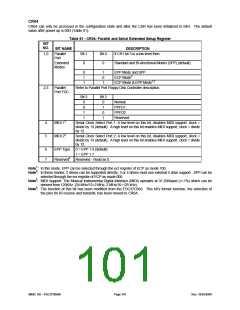
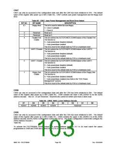
CR06
CR06 can only be accessed in the configuration state and after the CSR has been initialized to 06H. The default
value of this register after power up is FFH (Table 84). CR06 holds the floppy disk drive type IDs for up to four floppy
disk drives (see section Drive Type ID, Bits 4 - 5 on page 25).
Table 84 - DR06: Drive Type ID Register
FDD3
FDD2
FDD1
FDD0
D7
D6
D5
D4
D3
D2
D1
D0
ID31
ID30
ID21
ID20
ID11
ID10
ID01
ID00
SMSC DS – FDC37N3869
Page 102
Rev. 10/25/2000

 SMSC [ SMSC CORPORATION ]