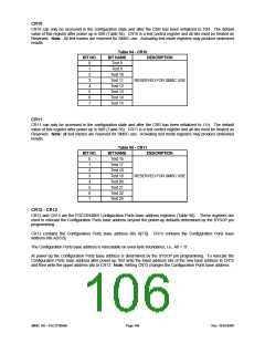
Setting either of the Force Disk Change bits active (1) forces the FDD nDSKCHG input active when the appropriate
drive has been selected. FORCE DSKCHG1 and FORCE DSKCHG0 can be written to a 1 but are not clearable by
software. FORCE DSKCHG1 is cleared on (nSTEP AND nDS1), FORCE DSKCHG0 is cleared on (nSTEP AND
nDS0). Note: The DSK CHG bit in the Floppy DIR register, Bit 7 = (nDS0 AND FORCE DSKCHG0) OR (nDS1 AND
FORCE DSKCHG1) OR nDSKCHG.
Force Write Protect, Bit 2
FORCE WRTPRT asserts the internal nWRTPRT input to the controller when the FORCE WRTPRT bit is active (“1”)
and a drive has been selected. The FORCE WRTPRT function applies to the nWRTPRT pin in the FDD Interface as
well as the nWRTPRT pin in the Parallel Port FDC.
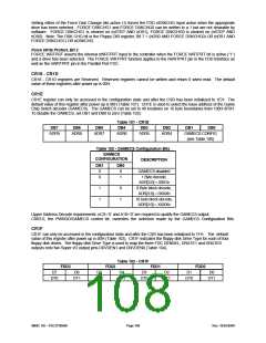
CR18 - CR1D
CR18 - CR1D registers are Reserved. Reserved registers cannot be written and return 0 when read. The default
value of these registers after power up is 00H.
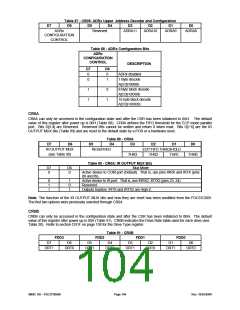
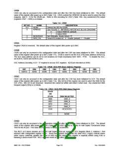
CR1E
CR1E register can only be accessed in the configuration state and after the CSR has been initialized to 1EH. The
default value of this register after power up is 80H (Table 101). CR1E is used to select the base address of the Game
Chip Select decoder (GAMECS). The GAMECS can be set to 48 locations on 16 byte boundaries from 100H-3F0H.
To disable the GAMECS, set DB1 and DB0 to zero (Table 102).
Table 101 - CR1E
DB7
DB6
DB5
DB4
DB3
DB2
DB1
DB0
ADR9
ADR8
ADR7
ADR6
ADR5
ADR4
GAMECS CONFIG
(see Table 100)
Table 102 - GAMECS Configuration Bits
GAMECS
CONFIGURATION
DESCRIPTION
DB1
0
0
DB0
0
1
GAMECS disabled
1 Byte decode,
ADR[3:0] = 0001b
8 Byte block decode,
ADR[3:0] = 0XXXb
16 byte block decode,
ADR[3:0] = XXXXb
1
1
0
1
Upper Address Decode requirements: nCS=’0’ and A10=’0’ are required to qualify the GAMECS output.
CR03.0, the PWRGD/GAMECS control bit, overrides the selection made by the GAMECS Configuration Bits.
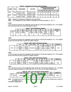
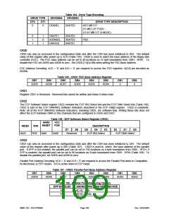
CR1F
CR1F can only be accessed in the configuration state and after the CSR has been initialized to 1FH. The default
value of this register after power up is 00H (Table 103). CR1F indicates the floppy disk Drive Type for each of four
floppy disk drives. The floppy disk Drive Type is used to map the three FDC DENSEL, DRATE1 and DRATE0
outputs onto two Super I/O output pins DRVDEN1 and DRVDEN0 (Table 104).
Table 103 - CR1F
FDD3
FDD2
FDD1
FDD0
D7
D6
D5
D4
D3
D2
D1
D0
DT0
DT1
DT0
DT1
DT0
DT1
DT0
DT1
SMSC DS – FDC37N3869
Page 108
Rev. 10/25/2000

 SMSC [ SMSC CORPORATION ]