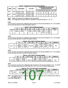
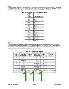
Table 96 - Configuration Ports Base Address Registers
CONFIGURATION PORTS BASE
ADDRESS REGISTERS
INDEX
0x122
R/W
HARD RESET
VCC POR
D7 D6 D5 D4 D3 D2 D1 D0
R/W SYSOP=0: 0xF0
SYSOP=1: 0x70
R/W
SYSOP=0: 0xF0
SYSOP=1: 0x70
SYSOP=0: 0x03
SYSOP=1: 0x03
A7 A6 A5 A4 A3
A2
A1 “0”
0x131
SYSOP=0: 0X03
SYSOP=1: 0x03
“0” “0” “0” “0” “0” A10 A9
A8
Note1: Writing CR13 changes the Configuration Ports base address.
Note2: The Configuration Ports Base Address is relocatable on even-byte boundaries; i.e., A0 = “0”.
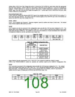
CR14
CR14 can only be accessed in the configuration state and after the CSR has been initialized to 14H. CR14 shadows
the bits in the write-only FDC run-time DSR register (Table 97).
Table 97 - CR14: DSR Shadow Register
D7
D6
D5
D4
D3
D2
D1
D0
DEFAULT
CR
14
R
SOFT
RESET
PWR
Res.
PRE-
PRE-
PRE-
DATA
RATE
SELECT
1
DATA
RATE
SELEC
T 0
N/A
DOWN
COMP COMP COMP
2
1
0
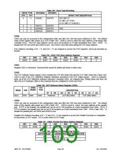
CR15
CR15 can only be accessed in the configuration state and after the CSR has been initialized to 15H. CR15 shadows
the bits in the write-only UART1 run-time FCR register (Table 98).
Table 98 - CR15: UART1 FCR Shadow Register
D7
D6
D5
D4
D3
D2
D1
D0
DEFAULT
XMIT
FIFO
RESE
T
RCVR
FIFO
RESE
T
RCVR
TRIGGER
MSB
RCVR
TRIGGE
R LSB
DMA
MODE
FIFO
ENABL
E
CR15
R
Reserved
N/A
SELECT
CR16
CR161 can only be accessed in the configuration state and after the CSR has been initialized to 16H. CR16 shadows
the bits in the write-only UART2 run-time FCR register (Table 99).
Table 99 - CR16: UART2 FCR Shadow Register
D7
D6
D5
D4
D3
D2
D1
D0
DEFAULT
RCVR
TRIGGE
R MSB
RCVR
TRIGGE
R LSB
DMA
XMIT
RCVR
MODE
FIFO
FIFO
FIFO
CR16
R
Reserved
N/A
SELECT RESET RESET
ENABLE
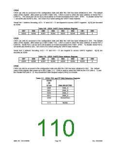
CR17
CR17 can only be accessed in the configuration state and after the CSR has been initialized to 17H. The default
value of this register after power up is 003H (Table 100). CR17 is the Force FDD Status Change register.
Table 100 - CR17: Force FDD Status Change Register
D7 D6 D5 D4
D3
D2
D1
D0
DEFAULT
CR
17
FORCE
FORCE
FORCE
R/W
RESERVED
RESERVE
D
WRTPRT DSKCHG1 DSKCHG0
0x03
Note: The controls in the Force FDD Status Change register (CR17) apply to the FDD Interface pins as well as to
the Parallel Port FDC.
Force Disk Change, Bits 0 - 1
SMSC DS – FDC37N3869
Page 107
Rev. 10/25/2000

 SMSC [ SMSC CORPORATION ]