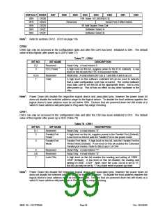
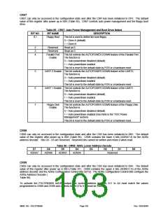
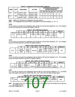
CR07
CR07 can only be accessed in the configuration state and after the CSR has been initialized to 07H. The default
value of this register after power up is 00H (Table 85). CR07 controls auto power management and the floppy boot
drive.
Table 85 - CR07: Auto Power Management and Boot Drive Select
BIT NO.
BIT NAME
DESCRIPTION
This bit is used to define the boot floppy.
0 = Drive A (default)
0,1
Floppy Boot
1 = Drive B
2
3
4
Reserved
Reserved
Read as 0.
Read as 0.
Parallel Port
This bit controls the AUTOPOWER DOWN feature of the Parallel Port.
Enable
The function is:
0 = Auto powerdown disabled (default)
1 = Auto powerdown enabled
This bit is reset to the default state by POR or a hardware reset.
5
6
7
UART 2 Enable This bit controls the AUTOPOWER DOWN feature of the UART2.
The function is:
0 = Auto powerdown disabled (default)
1 = Auto powerdown enabled
This bit is reset to the default state by POR or a hardware reset.
UART 1 Enable This bit controls the AUTOPOWER DOWN feature of the UART1.
The function is:
0 = Auto powerdown disabled (default)
1 = Auto powerdown enabled
This bit is reset to the default state by POR or a hardware reset.
Floppy Disk
Enable
This bit controls the AUTOPOWER DOWN feature of the Floppy Disk.
The function is:
0 = Auto powerdown disabled (default)
1 = Auto powerdown enabled (See Note in the “FDC Power
Management” section)
This bit is reset to the default state by POR or a hardware reset.
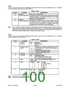
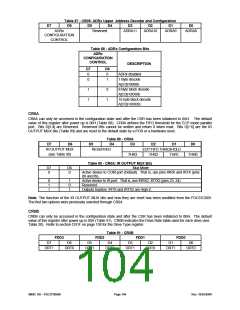
CR08
CR08 can only be accessed in the configuration state and after the CSR has been initialized to 08H. The default
value of this register after power up is 00H (Table 86). CR08 contains the lower 4 bits (ADRA7:4) for the ADRx
address decoder. Bits D0 - D3 are Reserved. Reserved bits cannot be written and return 0 when read.
Table 86 - CR08: ADRx Lower Address Decode
D7
D6
D5
D4
D3
D2
D1
D0
ADRA7
ADRA6
ADRA5
ADRA4
Reserved
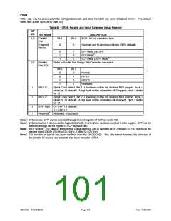
CR09
CR09 can only be accessed in the configuration state and after the CSR has been initialized to 09H. The default
value of this register after power up is 00H (Table 87). CR09 contains the upper 4 bits (ADRA11:8) of the ADRx
address decoder and the ADRx Configuration Control Bits D[7:6]. The ADRx Configuration Control Bits configure the
ADRx Address Decoder (
Table 88).
To activate the FDC37N3869 nADRx output, the system address bus bits A11 to A4 must match the values
programmed in CR08 and CR09 and address bits A12 to A15 must be ‘0000b’.
SMSC DS – FDC37N3869
Page 103
Rev. 10/25/2000

 SMSC [ SMSC CORPORATION ]