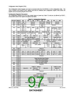
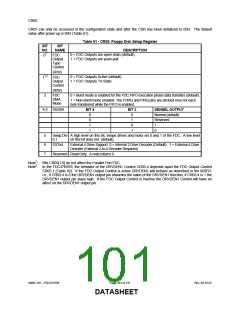
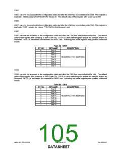
CR05
CR05 can only be accessed in the configuration state and after the CSR has been initialized to 05H. The default
value after power up is 00H (Table 81).
Table 81 - CR05: Floppy Disk Setup Register
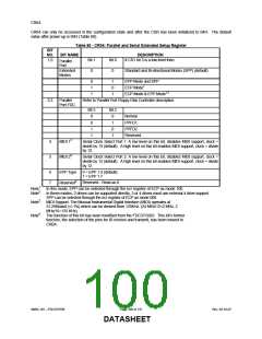
BIT
BIT
NO.
NAME
FDC
DESCRIPTION
0 = FDC Outputs are open drain (default).
01
Output
Type
1 = FDC Outputs are push-pull.
Control
(R/W)
11,2 FDC
0 = FDC Outputs Active (default).
1 = FDC Outputs Tri-State.
Output
Control
(R/W)
2
FDC
DMA
Mode
0 = Burst mode is enabled for the FDC FIFO execution phase data transfers (default).
1 = Non-Burst mode enabled. The FDRQ and FIRQ pins are strobed once for each
byte transferred while the FIFO is enabled.
4,3 DenSel
BIT 4
BIT 3
DENSEL OUTPUT
0
0
1
1
0
1
0
1
Normal (default)
Reserved
1
0
5
6
7
Swap Drv A high level on this bit, swaps drives and motor sel 0 and 1 of the FDC. A low level
0,1
on this bit does not (default).
EXTx4
External 4 Drive Support: 0 = Internal 2 Drive Decoder (Default). 1 = External 4 Drive
Decoder (External 2-to-4 Decoder Required).
Reserved Read Only. A read returns 0.
Note1: Bits CR05[1:0] do not affect the Parallel Port FDC.
Note2: In the FDC37N769, the behavior of the DRVDEN1 Control CR03.4 depends upon the FDC Output Control
CR05.1 (Table 82). If the FDC Output Control is active DRVDEN1 will behave as described in the 669FR;
i.e., if CR03.4 is 0 the DRVDEN1 output pin assumes the value of the DRVDEN1 function, if CR03.4 is 1 the
DRVDEN1 output pin stays high. If the FDC Output Control is inactive the DRVDEN1 Control will have no
affect on the DRVDEN1 output pin.
SMSC DS – FDC37N769
Page 101 of 137
Rev. 02-16-07
DATASHEET

 SMSC [ SMSC CORPORATION ]