Legacy-Free Keyboard/Embedded Controller with SPI and LPC Docking Interface
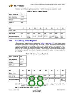
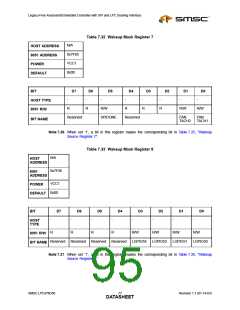
Table 7.26 Wakeup Source Register 8
N/A
HOST ADDRESS
8051 ADDRESS
POWER
0x7F55
VCC1
0x00
DEFAULT
BIT
D7
D6
D5
D4
D3
D2
D1
D0
-
-
-
-
-
-
-
-
HOST TYPE
8051 TYPE
BIT NAME
R
R
R
R
R/WC
R/WC
R/WC
R/WC
Reserved
Reserved Reserved Reserved LGPIO53 LGPIO52 LGPIO51 LGPIO50
Note 7.31 The interrupt source bits in this register are cleared by a writing a “1” to the bit. When an
interrupt source is asserted, a read from the corresponding bit in this register is a logic ‘1’.
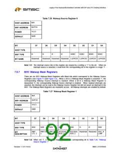
7.9.7
8051 Wakeup Mask Registers
There are six 8051 Wakeup Mask Registers with Mask bits which correspond to the Wakeup Source
Registers (see Figure 7.4 and Figure 7.5). When a bit in a Wakeup Mask Register is asserted ‘1’, the
corresponding Wakeup Source interrupt is masked. When a bit in a Wakeup Mask Register is
deasserted ‘0’, the corresponding Wakeup Source interrupt is enabled. When masked interrupts are
asserted, the interrupt can be read in the Wakeup Source Register but will not assert an interrupt to the
8051. The Wakeup Mask Registers are read/write access. All Wakeup interrupts are enabled by default.
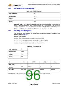
Table 7.27 Wakeup Mask Register 1
N/A
HOST ADDRESS
8051 ADDRESS
POWER
0x7F2C
VCC1
0x00
DEFAULT
BIT
D7
D6
D5
D4
D3
D2
D1
D0
-
-
-
-
-
-
-
-
HOST TYPE
8051 TYPE
R/W
R/W
R/W
R/W
R/W
R
R
R/W
PM1
PM1 EN PM1 STS ACCESS.
BUS 1
ACCESS. Reserved Reserved RTC_A
BUS 2 LRM
BIT
CTL 2
2
2
DESCRIPTION
Note 7.32 When set ‘1’, a bit in this register masks the corresponding bit in Table 7.20, "Wakeup
Source Register 1".
Revision 1.1 (01-14-03)
SMSC LPC47N350
DATA7S4HEET

 SMSC [ SMSC CORPORATION ]