Legacy-Free Keyboard/Embedded Controller with SPI and LPC Docking Interface
The bits in the INT1 Mask register are read/write. The INT1 interrupts are enabled by default.
Table 7.19 8051 INT1 Mask Register
N/A
HOST ADDRESS
8051 ADDRESS
POWER
0x7F03
VCC1
0x00
DEFAULT
BIT
D7
D6
D5
D4
D3
D2
D1
D0
-
-
-
-
-
-
-
-
HOST TYPE
8051 TYPE
R/W
IBF
R/W
R/W
R/W
R/W
R/W
R/W
R/W
KBD
EC_IBF EC_OBF GPIO3
I2C_SMB SYS-
US 1 MBOX
ANY
BIT DESCRIPTION
SCAN
WUP
7.9.6
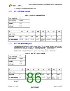
8051 Wakeup Source Registers
There are six 8051 Wakeup Source Registers (see Figure 7.4 and Figure 7.5). Each Wakeup Source
Register has eight Wakeup Source inputs which are logically ‘OR’ed to drive the 8051 external interrupt
1 input (int1_n) and the WAKE interrupt (int5_n). When a Wakeup Source input is asserted ‘1’ in a
Wakeup Source Register, an interrupt has occurred and, assuming the interrupt is enabled, the 8051
int1_n and int5_n inputs are asserted. A read from a Wakeup Source Register indicates the status of
the Wakeup Source inputs. Generally, the Wakeup Source bits in this register are cleared by a writing
a “1” to the bit.
Table 7.20 Wakeup Source Register 1
N/A
HOST ADDRESS
8051 ADDRESS
POWER
0x7F2A
VCC1
0x00
DEFAULT
BIT
D7
D6
D5
D4
D3
D2
D1
D0
-
-
-
-
-
-
-
-
HOST TYPE
8051 TYPE
R/WC
R/WC
R/WC
R/WC
R/WC
R
R
R/WC
PM1 CTL 2 PM1 EN PM1
STS 2
ACCESS. ACCESS. Reserved Reserved RTC_AL
BIT DESCRIPTION
2
BUS 1
BUS 2
RM
asserted
Note 7.25 The interrupt source bits in this register are cleared by a writing a “1” to the bit. When
asserted, a read from a bit in this register is a logic ‘1’.
PM1 CTL 2, PM1 EN 2, PM1 STS 2 [D7:D5]
Revision 1.1 (01-14-03)
SMSC LPC47N350
DATA7S0HEET

 SMSC [ SMSC CORPORATION ]