Legacy-Free Keyboard/Embedded Controller with SPI and LPC Docking Interface
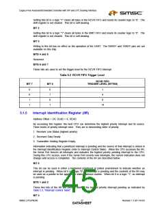
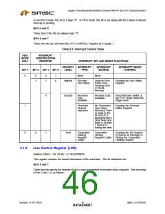
In non-FIFO mode, this bit is a logic "0". In FIFO mode, this bit is set along with bit 2 when a timeout
interrupt is pending.
BITS 4 and 5
These bits of the IIR are always logic "0".
BITS 6 and 7
These two bits are set when the FIFO CONTROL Register bit 0 equals 1.
Table 5.3 Interrupt Control Table
FIFO
MODE
ONLY
INTERRUPT
IDENTIFICATION
REGISTER
INTERRUPT SET AND RESET FUNCTIONS
PRIORITY
LEVEL
INTERRUPT
TYPE
INTERRUPT
SOURCE
INTERRUPT RESET
CONTROL
BIT 3
BIT 2
BIT 1
BIT 0
0
0
1
0
1
1
0
-
None
None
-
Highest
Receiver
Overrun Error,
Parity Error,
Framing Error
or Break
Reading the Line Status
Register
Line Status
Interrupt
0
Second
Received
Data
Receiver Data
Available
Read Receiver Buffer or
the FIFO drops below the
trigger level.
Available
1
Character
Timeout
No Characters
Have Been
Reading the Receiver
Buffer Register
Indication
Removed From
or Input to the
RCVR FIFO
during the last 4
Char times and
there is at least
1 char in it
during this time
0
0
1
Third
Transmitter
Holding
Transmitter
Holding
Reading the IIR Register
(if Source of Interrupt) or
Writing the Transmitter
Holding Register
Register
Empty
Register Empty
5.1.6
Line Control Register (LCR)
Address Offset = 3H, DLAB = 0, READ/WRITE
This register contains the format information of the serial line. The bit definitions are:
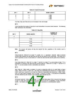
BITS 0 and 1
These two bits specify the number of bits in each transmitted or received serial character. The encoding
of bits 0 and 1 is as follows:
Revision 1.1 (01-14-03)
SMSC LPC47N350
DATA2S8HEET

 SMSC [ SMSC CORPORATION ]