Legacy-Free Keyboard/Embedded Controller with SPI and LPC Docking Interface
Chapter 29 Timing Diagrams
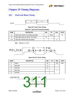
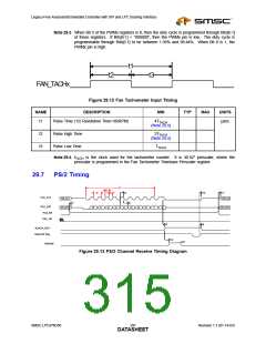
29.1
Clock and Reset Timing
t1
t2
t2
CLOCKI
Figure 29.1 Input Clock Timing
Table 29.1 Input Clock Timing Parameters
NAME
DESCRIPTION
MIN
TYP
MAX
UNITS
t1
t2
Clock Cycle Time for 14.318 MHz (See Note)
Clock High Time/Low Time for 14.318 MHz
Clock Rise Time/Fall Time (not shown)
69.84
ns
15
tr, tf
5
Note: Tolerance is ± 0.01%.
t1
t4
P C I_C LK
t3
Figure 29.2 PCI Clock Timing
DESCRIPTION
NAME
MIN
TYP
MAX
UNITS
t1
t2
t3
t4
t5
Period
30
12
12
33.3
nsec
High Time
Low Time
Rise Time
Fall Time
3
t1
L R E S E T #
Figure 29.3 Reset Timing
SMSC LPC47N350
293
Revision 1.1 (01-14-03)
DATASHEET

 SMSC [ SMSC CORPORATION ]