Legacy-Free Keyboard/Embedded Controller with SPI and LPC Docking Interface
Table 27.4 Global Configuration Registers (continued)
REGISTER
ADDRESS
DESCRIPTION
CHIP (GLOBAL) CONTROL REGISTERS
Device Mode
0x25 R/W
Bit [1-0] Reserved – writes ignored, reads return “0”.
Bit[2] SerIRQ Mode (Note 27.5)
= 0: Serial IRQ Disabled.
= 1: Serial IRQ Enabled
(Default).
Bit [7:3] Reserved – writes ignored, reads return “0”.
Registers Base
Address
0x26-0x27
See Section 27.2.3, "Base Address Configuration Registers".
Test Registers
TEST 0
0x28-0x2B
0x2C
SMSC Test Mode Registers, Reserved for SMSC.
Test Modes - Reserved for SMSC. Users should not write to this
register, may produce undesired results.
TEST 1
TEST 2
TEST 3
0x2D R/W
0x2E R/W
0x2F R/W
Test Modes: Reserved for SMSC. Users should not write to this
register; may produce undesired results.
Test Modes - Reserved for SMSC. Users should not write to this
register; may produce undesired results.
Test Modes - Reserved for SMSC. Users should not write to this
register; may produce undesired results.
Note 27.5 The SerIRQ Mode bit controls the SER_IRQ pin and the CLKRUN# pin. (see Section 24.2,
"Using CLKRUN#").
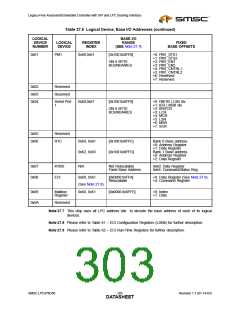
27.4
Logical Device Configuration/Control Registers [0x30-0xFF]
Used to access the registers that are assigned to each logical unit. This chip supports ten logical units
and has ten sets of logical device registers:
■
■
■
■
■
■
PM1
Serial
Real Time Clock
Keyboard Controller
Embedded Controller
Mailbox Interface
A separate set (bank) of control and configuration registers exists for each Logical Device and is
selected with the Logical Device # Register (0x07). The INDEX PORT is used to select a specific logical
device register. These registers are then accessed through the DATA PORT. The Logical Device
registers are accessible only when the device is in the Configuration State The logical register
addresses are listed in Table 27.5.
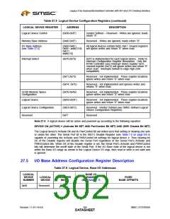
Table 27.5 Logical Device Configuration Registers
LOGICAL DEVICE REGISTER
ADDRESS
(0x30)
DESCRIPTION
Activate
Bits[7:1] Reserved, set to “0”.
Bit[0]
= 1 Activates the logical device currently selected
through the Logical Device # register.
= 0 Logical device currently selected is inactive.
Logical Device Control
SMSC LPC47N350
(0x31-0x37)
Reserved - Writes are ignored, reads return “0”.
283
Revision 1.1 (01-14-03)
DATASHEET

 SMSC [ SMSC CORPORATION ]