Legacy-Free Keyboard/Embedded Controller with SPI and LPC Docking Interface
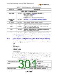
Table 27.5 Logical Device Configuration Registers (continued)
LOGICAL DEVICE REGISTER
ADDRESS
DESCRIPTION
Logical Device Control
(0x38-0x3F)
Vendor Defined – Reserved - Writes are ignored, reads
return “0”.
Memory Base Address
(0x40-0x5F)
Reserved - Writes are ignored, reads return “0”.
I/O Base Address
(see Table 27.6)
(0x60-0x6F)
0x60= addr[15:8]
0x61=
All logical devices contain 0x60, 0x61. Unused registers
will ignore writes and return “0” when read.
addr[7:0]
Interrupt Select
(0x70,0x72)
0x70 is implemented for each logical device. Refer to
Interrupt Configuration Register description. Only the
KYBD controller uses Interrupt Select register 0x72.
Unused register (0x72) will ignore writes and return “0”
when read. Interrupts default to edge high (ISA
compatible).
(0x71,0x73)
(0x74, 0x75)
(0x76-0xA8)
(0xA9-0xDF)
(0xE0-0xFE)
0xFF
Reserved - not implemented. These register locations
ignore writes and return “0” when read.
Reserved - not implemented and ignores writes and
returns “0” when read.
32-Bit Memory Space
Configuration
Reserved - not implemented. These register locations
ignore writes and return “0” when read.
Logical Device
Reserved - not implemented. These register locations
ignore writes and return “0” when read.
Logical Device Configuration
Reserved
Reserved - Vendor Defined (see SMSC defined Logical
Device Configuration Registers).
Reserved
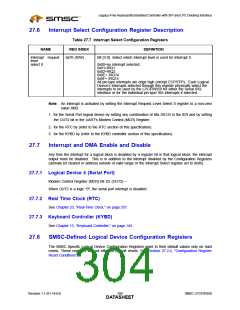
Note 27.6 A logical device will be active and powered up according to the following equation:
DEVICE ON (ACTIVE) = (Activate Bit SET AND Pwr/Control Bit SET) AND (8051 Disable Bit SET)
The Logical device's Activate Bit and its Pwr/Control Bit are linked such that setting or clearing one sets
or clears the other. The Serial Port bit in the 8051’s Disable Register (see Table 7.8 on page 59) is
capable of overriding the Activate and PWR/Control bit settings for logical device 4. Thus clearing bit
D6 of the Disable register will disable the Serial Port regardless of the Serial Port’s Activate and
PWR/Control bits. When D6 of the Disable register is set, the Serial Port’s Activate and PWR/Control
bits will determine the on/off state of the Serial Port. If the I/O Base Addr of the logical device is not
within the Base I/O range as shown in the Logical Device I/O map, then read or write is not valid and
is ignored.
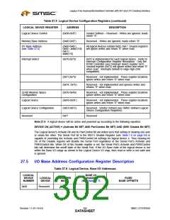
27.5
I/O Base Address Configuration Register Description
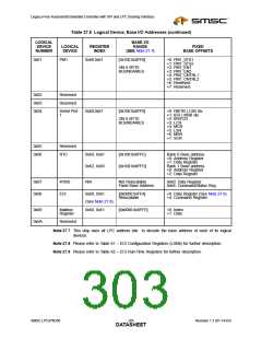
Table 27.6 Logical Device, Base I/O Addresses
BASE I/O
LOGICAL
DEVICE
LOGICAL
DEVICE
REGISTER
INDEX
RANGE
FIXED
NUMBER
(SEE Note 27.7)
BASE OFFSETS
0x00
Reserved
Revision 1.1 (01-14-03)
284
SMSC LPC47N350
DATASHEET

 SMSC [ SMSC CORPORATION ]