Legacy-Free Keyboard/Embedded Controller with SPI and LPC Docking Interface
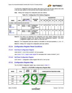
To relocate the configuration ports base address after power-up, first write the lower address byte (LSB)
of the new base address to CR26 and then write the upper address bits to CR27.
Note: Writing CR27 changes the configuration ports base address.
Table 27.2 Configuration Port Address Registers
DESCRIPTION
HARD RESET
REGISTER
NAME
INDEX
TYPE
(SEE Note 27.2)
D7 D6 D5 D4
D3
D2
D1 D0
GLOBAL CONFIGURATION REGISTERS
0x26
R/W
MODE = 0: 0x2E Configuration
MODE = 1: 0x4E Port Base
Address Byte 0
A7
“0”
A6 A5 A4
A3
A2
A1 “0”
(See
Note 27.3)
(LSB)
0x27
R/W
MODE = 0: 0x00 Configuration
MODE = 1: 0x00 Port Base
Address Byte 1
“0” “0” “0” A11 A10 A9 A8
(See
Note 27.4)
(MSB)
Note 27.2 The MODE pin determines the configuration port base address following Hard Reset
Configuration Register (See Section Hard Reset Configuration Register). Soft Reset
Configuration Register has no effect on CR26 and CR27
Note 27.3 The configuration ports base address is relocatable on even-byte boundaries; i.e., A0 = “0”.
Note 27.4 Writing CR27 changes the configuration ports base address.
27.2.4 Configuration Register Reset Conditions
27.2.4.1 Hard Reset Configuration Register
HARD RESET = VCC2 POR or nRESET_OUT pin asserted.
(See Section 7.8.3.5, "Output Enable Register" for description 8051 control of nRESET_OUT)
27.2.4.2 Soft Reset Configuration Register
SOFT RESET = Configuration Control Register Bit0 set to a one by host.
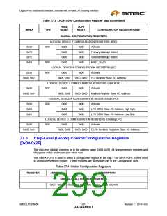
27.2.5 Configuration Register Map
The LPC47N350 Configuration register map is shown below in Table 27.1.
Table 27.3 LPC47N350 Configuration Register Map
HARD
SOFT
INDEX
TYPE
RESET
RESET
CONFIGURATION REGISTER NAME
GLOBAL CONFIGURATION REGISTERS
0x02
0x03
0x07
0x17
W
0x00
0x00
Config Control
RESERVED
-
R/W
-
-
0x00
-
-
0x00
-
Logical Device Number
RESERVED
SMSC LPC47N350
279
Revision 1.1 (01-14-03)
DATASHEET

 SMSC [ SMSC CORPORATION ]