Legacy-Free Keyboard/Embedded Controller with SPI and LPC Docking Interface
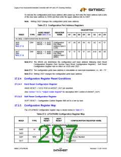
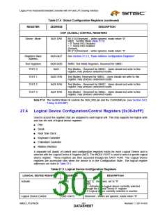
Table 27.3 LPC47N350 Configuration Register Map (continued)
HARD
RESET
SOFT
RESET
INDEX
TYPE
CONFIGURATION REGISTER NAME
GLOBAL CONFIGURATION REGISTERS
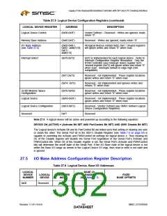
LOGICAL DEVICE 7 CONFIGURATION REGISTERS (KBD)
0x30
0x70
0x72
0xF0
R/W
0x00
0x00
0x00
0x00
0x00
0x00
0x00
0x00
Activate
Primary Interrupt Select
Second Interrupt Select
KRST_GA20
R/W
R/W
LOGICAL DEVICE 8 CONFIGURATION REGISTERS (EC)
0x30
0x00
0x00
Activate
0x60, 0x61
0x00, 0x62
0x00, 0x62
ECI Register Base I/O Address
LOGICAL DEVICE 9 CONFIGURATION REGISTERS (MAILBOX)
0x30
R/W
0x00
0x00
Activate
0x60, 0x61
0x00, 0x00
0x00, 0x00
Mailbox Register Base I/O Address
LOGICAL DEVICE A CONFIGURATION REGISTERS (LGPIO)
0x30
0x60
0x61
R/W
0x00
0x00
0x00
0x00
0x00
0x00
Activate
LPC GPIO Base I/O Address High Byte
LPC GPIO Base I/O Address Low Byte
LOGICAL DEVICE C CONFIGURATION REGISTERS (Docking LPC)
0x30
R/W
0x00
0x00
Activate
0x60, 0x61
0x00, 0x00
0x00, 0x00
DLPC Runtime Registers Base I/O Address
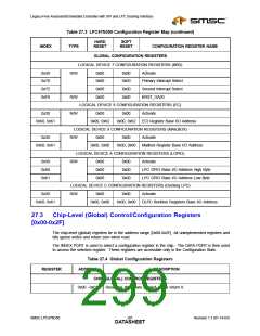
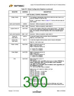
27.3
Chip-Level (Global) Control/Configuration Registers
[0x00-0x2F]
The chip-level (global) registers lie in the address range [0x00-0x2F]. All unimplemented registers and
bits ignore writes and return zero when read.
The INDEX PORT is used to select a configuration register in the chip. The DATA PORT is then used
to access the selected register. These registers are accessible only in the Configuration State.
Table 27.4 Global Configuration Registers
REGISTER
ADDRESS
DESCRIPTION
CHIP (GLOBAL) CONTROL REGISTERS
0x00 –0x01
Reserved, Writes are ignored, reads return 0.
SMSC LPC47N350
281
Revision 1.1 (01-14-03)
DATASHEET

 SMSC [ SMSC CORPORATION ]