Legacy-Free Keyboard/Embedded Controller with SPI and LPC Docking Interface
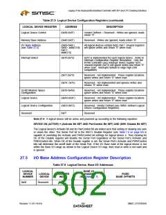
Table 27.6 Logical Device, Base I/O Addresses (continued)
LOGICAL
DEVICE
BASE I/O
RANGE
(SEE Note 27.7)
LOGICAL
DEVICE
REGISTER
INDEX
FIXED
NUMBER
BASE OFFSETS
0x01
PM1
0x60,0x61
[0x100:0x0FF8]
+0: PM1_STS1
+1: PM1_STS2
+2: PM1_EN1
+3: PM1_EN2
+4: PM1_CNTRL1
+5: PM1_CNTRL2
+6: Reserved
ON 8 BYTE
BOUNDARIES
+7: Reserved
0x02
0x03
0x04
Reserved
Reserved
Serial Port
1
0x60,0x61
[0x100:0x0FF8]
+0: RB/TB | LSB div
+1: IER | MSB div
+2: IIR/FCR
+3: LCR
ON 8 BYTE
BOUNDARIES
+4: MCR
+5: LSR
+6: MSR
+7: SCR
0x05
0x06
Reserved
RTC
0x60, 0x61
0x62, 0x63
[0x100:0x0FFE]
[0x100:0x0FFD]
Bank 0 Base address
+0: Address Register
+1: Data Register
Bank 1 Base address
+0: Address Register
+2: Data Register
0x07
0x08
KYBD
ECI
N/A
Not Relocatable
0x60: Data Register
Fixed Base Address
0x64: Command/Status Reg.
0x60, 0x61
[0x0000:0xFFA]
Relocatable
+0: Data Register (See Note 27.9)
+4: Command Register
(See Note 27.8)
0x60, 0x61
0x09
0x0A
Mailbox
Register
[0x0000:0x0FFE]
+0: Index
+1: Data
Reserved
Note 27.7 This chip uses all LPC address bits to decode the base address of each of its logical
devices.
Note 27.8 Please refer to Table 61 – ECI Configuration Registers (LDN8) for further description.
Note 27.9 Please refer to Table 62 – ECI Run-Time Registers for further description.
SMSC LPC47N350
285
Revision 1.1 (01-14-03)
DATASHEET

 SMSC [ SMSC CORPORATION ]