Legacy-Free Keyboard/Embedded Controller with SPI and LPC Docking Interface
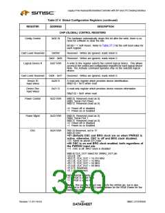
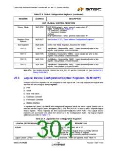
Table 27.4 Global Configuration Registers (continued)
REGISTER
ADDRESS
DESCRIPTION
CHIP (GLOBAL) CONTROL REGISTERS
Config Control
0x02 W
The hardware automatically clears this bit after the write; there is no
need for software to clear the bits.
Bit [0] = 1: Soft Reset; Refer to Table 27.3 for the soft reset value for
each register.
Card Level Reserved
Logical Device #
0x03W
Reserved - Writes are ignored, reads return 0.
Reserved - Writes are ignored, reads return 0.
0x04 - 0x06
0x07 R/W
A write to this register selects the current logical device. This allows
access to the control and configuration registers for each logical device.
Note: The Activate command operates only on the selected logical
device.
Card Level Reserved
0x08 - 0x1F
0x20 R
Reserved - Writes are ignored, reads return 0.
Device ID
A read-only register which provides device identification.:
Bits[7-0] = 0x15 when read
Hard Wired
Device Rev
Hard Wired
0x21 R
A read-only register which provides device revision information.
Bits[7-0] = 0x01 when read
Power Control
0x22 R/W
Bit[0:3] Reserved (read as 0)
Bit[4] Serial Port Power
Bit[5:7] Reserved (read as 0)
=0 Power off or disabled
=1 Power on or Enabled
Power Mgmt
OSC
0x23 R/W
0x24 R/W
Bit[0:3] Reserved (read as 0)
Bit[4] Serial Port 1
Bit[5:7] Reserved (read as 0)
=0 Power off or disabled
=1 Power on or Enabled
Bit[1:0] Reserved, set to “0”
Bit[3:2] OSC
=01 (default) OSC and BRG clock are on when PWRGD is
active, otherwise, OSC is off and BRG clock disabled.
=10 Same as above (01) case
=00 OSC is on and BRG clock enabled, both regardless of
the PWRGD input pin.
=11 OSC is off, BRG Clock is disabled
Bit[6:4] CLK_OUT Select for 24MHz_OUT pin
=[0,0,0] Off
=[0,0,1] CLK_OUT = 14.318 MHz
=[0,1,0] CLK_OUT = 16 MHz
=[0,1,1] CLK_OUT = 24 MHz
=[1,0,0] CLK_OUT = 48 MHz
=[1,0,1] Reserved
=[1,1,X] Reserved
Bit[7] nIRQ8 Polarity
=0 nIRQ8 is active high
=1 nIRQ8 is active low
Note: This polarity bit not only affects the nIRQ8 pin, but is also
reflected in the Serial IRQ sample phase for the IRQ8 Frame for the
Serial IRQ Bus.
Revision 1.1 (01-14-03)
282
SMSC LPC47N350
DATASHEET

 SMSC [ SMSC CORPORATION ]