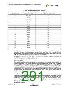
Legacy-Free Keyboard/Embedded Controller with SPI and LPC Docking Interface
Chapter 27 LPC47N350 Configuration
27.1
Overview
The Configuration of the LPC47N350 is very flexible and is based on the configuration architecture
implemented in typical Plug-and-Play components.
The LPC47N350 is designed for motherboard designs in which the resources required by their
components are known. With its flexible resource allocation architecture, the LPC47N350 allows the
BIOS to assign resources at POST.
27.2
Configuration Register Access
Only two states are defined (Run and Configuration). In the Run State, the chip will always be ready
to enter the Configuration State.
The desired configuration registers are accessed in two steps:
a. Write the index of the Logical Device Number Configuration Register (i.e., 0x07) to the INDEX PORT
and then write the number of the desired logical device to the DATA PORT.
b. Write the address of the desired configuration register within the logical device to the
INDEX PORT and then write or read the configuration register through the DATA PORT.
Note: If accessing the Global Configuration Registers, step (a) is not required.
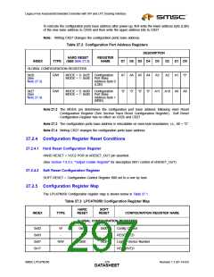
27.2.1 Primary Configuration Address Decoder
The logical devices are configured through three Configuration Access Ports (CONFIG, INDEX and
DATA). The BIOS uses these ports to initialize the logical devices at POST (Table 27.1).
The MODE pin is a hardware configuration pin that sets the default Configuration Access Port base
address at power-up. The status of the mode pin can be read by the 8051 through the Led Register
(MMCR 7F21h). See Section 7.8.4, "LED Controls," on page 63. The Configuration Ports base address
can also be changed using the configuration ports base address register (see Section 27.2.3, "Base
Address Configuration Registers").
Table 27.1 LPC47N350 Configuration Access Ports
MODE PIN = 0
(10K PULL-DOWN RESISTOR
OR TIE TO GND)
MODE PIN = 1
(10K PULL-UP RESISTOR OR
TIE TO VCC1)
PORT NAME
TYPE
CONFIG PORT
INDEX PORT
DATA PORT
0x02E
0x04E
Write
Read/Write
INDEX PORT + 1
Note 27.1 This address can be changed by configuration registers 26h and 27h.
27.2.1.1 Entering the Configuration State
The INDEX and DATA ports are effective only when the chip is in the Configuration State. The device
enters the Configuration State when the following Config Key is successfully written to the CONFIG
PORT.
Config Key = < 0x55>
SMSC LPC47N350
277
Revision 1.1 (01-14-03)
DATASHEET

 SMSC [ SMSC CORPORATION ]