Legacy-Free Keyboard/Embedded Controller with SPI and LPC Docking Interface
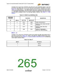
The MISC18 bit is used in the LPC47N350, along with bit D3 in the ESMI Mask register to select the
pin function and buffer mode for the OUT7 pin and the SMI transfer mechanism to the host.
(Table 21.19). When MISC18 = ‘0’, the primary function of the OUT7 pin is selected and the SMI is
routed to the Serial IRQ interface. If the SMI is masked, SIRQ slot3 is available as IRQ2. When MISC18
= ‘1’, the alternate nSMI function of the OUT7 pin is selected, the pad is driven open-drain, and the
Serial IRQ slot3 is available as IRQ2. The ESMI Mask register IS MBX97h. See Section 17.7, "ESMI
Registers".
Table 21.19 MISC18 and ESMI Mask Bits
ESMI MASK
REGISTER
D3
FUNCTION
DESCRIPTION
MISC18
OUT7 PIN
SIRQ SLOT3
0
0
0
1
OUT7
nSMI
nSMI
IRQ2
SERIAL SMI (DEFAULT)
PARALLEL SMI, SERIAL IRQ IRQ2
AVAILABLE
1
1
0
1
OUT7
nSMI
IRQ2
IRQ2
MASKED SERIAL SMI, IRQ2
AVAILABLE
PARALLEL SMI MASKED
(INACTIVE), IRQ2 AVAILABLE
MISC17 – D1
The MISC17 bit is used in the LPC47N350 to select the pin function and buffer mode between KSO13
and GPIO18 on pin KSO13 (Table 21.20). MISC17 also affects the multiplex functions for the OUT8,
KSO12 and KSO13 pins (see Section 21.2, "Functions Available on More than One Pin" for Multiplexing
control register interactive effects).
Table 21.20 Misc17
MISC17
PIN KSO13
0
1
KSO13
GPIO18
SMSC LPC47N350
247
Revision 1.1 (01-14-03)
DATASHEET

 SMSC [ SMSC CORPORATION ]