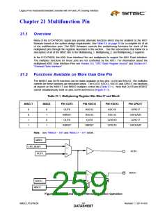
Legacy-Free Keyboard/Embedded Controller with SPI and LPC Docking Interface
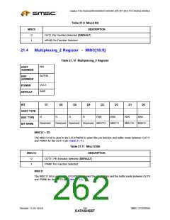
Table 21.9 Misc0 Bit
DESCRIPTION
MISC0
0
1
OUT1 Pin Function Selected (DEFAULT)
nIRQ8 Pin Function Selected
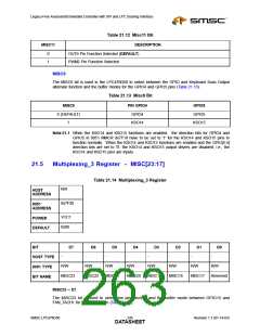
21.4
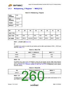
Multiplexing_2 Register - MISC[16:9]
Table 21.10 Multiplexing_2 Register
N/A
HOST
ADDRESS
0x7F40
8051
ADDRESS
VCC1
0x00
POWER
DEFAULT
BIT
D7
D6
D5
D4
D3
D2
D1
D0
-
-
-
-
-
-
-
-
HOST TYPE
8051 TYPE
BIT NAME
R
R
R
R
R/W
R/W
R/W
R/W
Reserved
Reserved Reserved Reserved MISC12
MISC11
MISC10
MISC9
MISC12 – D3
The MISC12 bit is used in the LPC47N350 to select the pin function and buffer mode between OUT11
and PWM1 for the OUT11 pin (Table 21.11).
Table 21.11 Misc12 Bit
MISC12
DESCRIPTION
OUT11 Pin Function Selected (DEFAULT)
PWM1 Pin Function Selected
0
1
MISC11
The MISC11 bit is used in the LPC47N350 to select the pin function and the buffer mode between OUT9
and PWM0 for the OUT9 pin (Table 21.12).
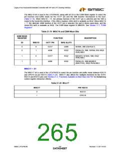
Revision 1.1 (01-14-03)
244
SMSC LPC47N350
DATASHEET

 SMSC [ SMSC CORPORATION ]