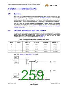
Legacy-Free Keyboard/Embedded Controller with SPI and LPC Docking Interface
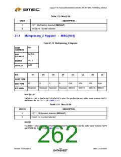
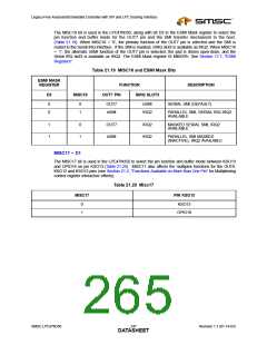
Table 21.12 Misc11 Bit
MISC11
DESCRIPTION
0
1
OUT9 Pin Function Selected (DEFAULT)
PWM2 Pin Function Selected
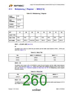
MISC9
The MISC9 bit is used in the LPC47N350 to select between the GPIO and Keyboard Scan Output
alternate function and the buffer modes for the GPIO4 and GPIO5 pins (Table 21.13).
Table 21.13 Misc9 Bit
MISC9
PIN GPIO4
GPIO5
0 (DEFAULT)
1
GPIO4
KSO14
GPIO5
KSO15
Note 21.1 When the KSO14 and KSO15 functions are enabled, the direction bits for GPIO4 and
GPIO5 in 8051 MMCR 0x7F18 have to be set to '1' for the KSO14 and KSO15 pins to
function normally. When the KSO14 and KSO15 functions are enabled and the GPIO[5:4]
direction bits are set to '0', the KSO14 and KSO15 output drivers are disabled; i.e., the
KSO14 and KSO15 pins are inputs.
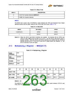
21.5
Multiplexing_3 Register - MISC[23:17]
Table 21.14 Multiplexing_3 Register
N/A
HOST
ADDRESS
0x7F30
8051
ADDRESS
VCC1
0x00
POWER
DEFAULT
BIT
D7
D6
D5
D4
D3
D2
D1
D0
-
-
-
-
-
-
-
-
HOST TYPE
8051 TYPE
BIT NAME
R/W
R/W
R/W
R/W
R/W
R/W
R/W
R/W
MISC23
MISC22
MISC21
MISC20
MISC19
MISC18
MISC17
Reserved
MISC23 – D7
The MISC23 bit is used to select the pin function and the buffer mode between GPIO15 and
FAN_TACH1 for the GPIO15 pin (Table 21.15).
SMSC LPC47N350
245
Revision 1.1 (01-14-03)
DATASHEET

 SMSC [ SMSC CORPORATION ]