Legacy-Free Keyboard/Embedded Controller with SPI and LPC Docking Interface
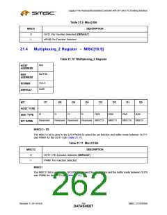
Table 21.5 Misc4 Bit
MISC4
DESCRIPTION
0
1
OUT10 Pin Function Selected (DEFAULT)
PWM0 Pin Function Selected
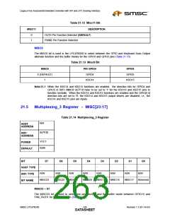
MISC3 – D3
The MISC3 bit is used to select between the nFDD_LED and the 8051RX alternate function and the
buffer mode (Table 21.6).
Table 21.6 Misc3 Bit
MISC3
DESCRIPTION
0
1
nFDD_LED (DEFAULT)
8051RX
MISC2 – D2
The MISC2 bit is used in to select between the nPWR_LED and 8051TX function (Table 21.7).
Table 21.7 Misc2 Bit
MISC2
DESCRIPTION
0
1
nPWR_LED (DEFAULT)
8051TX
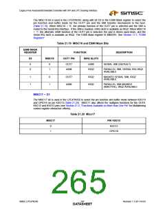
MISC1 – D1
The MISC1 bit is used to select the pin function and the buffer mode between GPIO20 and GPIO21,
and the PS/2 CLK and DATA (Table 21.8).
Table 21.8 Misc1 Bit
MISC[1]
PIN GPIO20
PIN GPIO21
0 (DEFAULT)
1
GPIO20
PS2CLK
GPIO21
PS2DAT
The PS/2 pins on GPIO20 and GPIO21 are disabled (internally pulled high) when the non-PS/2 alternate
functions are selected. The PS/2 inputs under this condition are seen as a high to the PS/2 Device
Interface logic.
Whenever a PS/2 channel is not enabled, the input signals to that channel must be high. The
LPC47N350 provides this through the use of weak pull-ups since the EM and KB channels share a
common receive path and the IM and PS2 channels also share a common receive path.
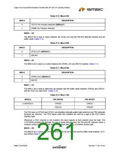
MISC0 – D0
The MISC0 bit is used in the LPC47N350 to select the pin function and the buffer mode between OUT1
and nIRQ8 (Table 21.9)
SMSC LPC47N350
243
Revision 1.1 (01-14-03)
DATASHEET

 SMSC [ SMSC CORPORATION ]