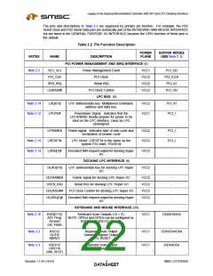
Legacy-Free Keyboard/Embedded Controller with SPI and LPC Docking Interface
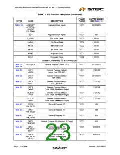
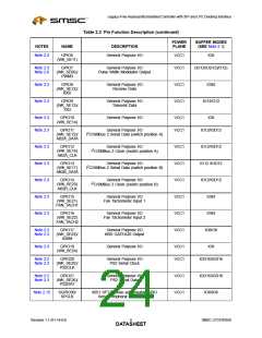
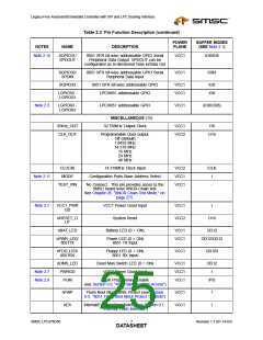
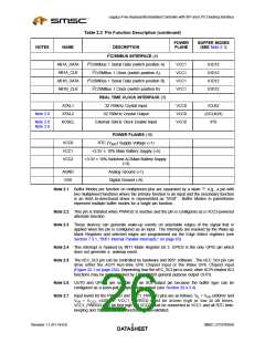
Table 2.2 Pin Function Description (continued)
POWER
BUFFER MODES
NOTES
NAME
DESCRIPTION
PLANE
(SEE Note 2.1)
I2C/SMBUS INTERFACE (4)
I2C/SMBus 1 Serial Data (switch position A)
I2C/SMBus 1 Clock (switch position A)
I2C/SMBus 1 Serial Data (switch position B)
I2C/SMBus 1 Clock (switch position B)
REAL TIME CLOCK INTERFACE (3)
32.768kHz Crystal Input
AB1A_DATA
AB1A_CLK
AB1B_DATA
AB1B_CLK
VCC1
VCC1
VCC1
VCC1
IOD12
IOD12
IOD12
IOD12
XTAL1
XTAL2
XOSEL
VCC0
VCC0
VCC0
ICLK2
(OCLK2/I)
IPD
Note 2.8
32.768kHz Crystal Output
Note 2.8
Note 2.9
External 32kHz Clock Enable Input
POWER PLANES (18)
RTC (VBAT) Supply Voltage (×1)
+3.3V ± 10% Main Battery Supply (×5)
VCC0
VCC1
VCC2
+3.3V ± 10% Switched AC/Main Battery Supply
(×3)
AGND
VSS
Analog Ground (×1)
Digital Ground (×8)
Note 2.1 Buffer Modes per function on multiplexed pins are separated by a slash “/”; e.g., a pin with
two multiplexed functions where the primary function is an input and the secondary function
is an 8mA bi-directional driver is represented as “I/IO8”. Buffer Modes in parenthesis
represent multiple buffer modes for a single pin function.
Note 2.2 This pin is tristated when PWRGD is inactive and the pin is configured as a VCC2-powered
alternate function.
Note 2.3 These devices can generate wake-up events on selectable edges of the signal that is
applied when the pin is configured as an input. The interrupts are masked by the Wake-up
Mask Registers and selected edges are programmed via the Edge Select registers (see
Section 7.9.1, "8051 Internal Parallel Interrupts," on page 65)
Note 2.4 This interrupt is masked by INT1 Mask Register bit 3. GPIO3 is the only GPIO pin which
does not generate a wakeup event.
Note 2.5 The nEC_SCI pin can be controlled by hardware and 8051 software. The nEC_SCI pin can
drive either the ACPI Run-time GPE Chipset input or the Wake GPE Chipset input
(Figure 22.1 on page 254). Depending how the nEC_SCI pin is used, other ACPI-related SCI
functions may be best supplied by LPC47N350 general purpose output OUT0.
Note 2.6 OUT0 and GPIO7 are suitable as an SCI output pin because the buffer type can be
configured as a push-pull or open-drain output (see Section 20.4.3.4)
Note 2.7 Input levels for the PWRGD and VCC1_PWRGD pins are as follows: VIL = VSS ±400mV and
VIH = VCC1 ±400mV. VCC1_PWRGD must be driven high or low at all times.
VCC1_PWRGD may be tied high but VCC0 must be connected to VCC1 and all RTC time-
keeping and CMOS memory functions are invalidated.
Revision 1.1 (01-14-03)
8
SMSC LPC47N350
DATASHEET

 SMSC [ SMSC CORPORATION ]