Legacy-Free Keyboard/Embedded Controller with SPI and LPC Docking Interface
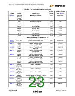
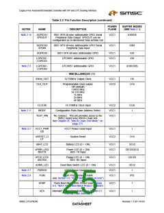
Table 2.2 Pin Function Description (continued)
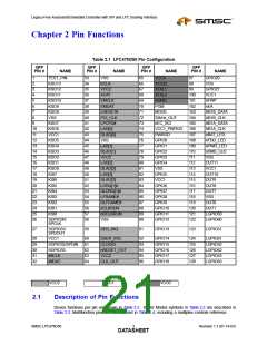
POWER
BUFFER MODES
NOTES
NAME
DESCRIPTION
PLANE
(SEE Note 2.1)
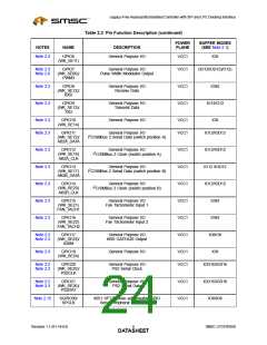
Note 2.3
GPIO6
General Purpose I/O
VCC1
IO8
(WK_SE11)
Note 2.3
Note 2.6
GPIO7
(WK_SE06)/
PWM3
General Purpose I/O
VCC1
VCC1
VCC1
(IO12/IOD12)/O12)
Pulse Width Modulator Output
Note 2.3
Note 2.3
GPIO8
(WK_SE12)/
RXD
General Purpose I/O
Receive Data
IO8/I
GPIO9
(WK_SE13)/
TXD
General Purpose I/O
Transmit Data
IO12/O12
Note 2.3
Note 2.3
GPIO10
General Purpose I/O
VCC1
VCC1
IO8
(WK_SE14)
GPIO11
General Purpose I/O
IO12/IOD12
(WK_SE15)/
AB2A_DATA
I2C/SMBus 2 Serial Data (switch position A)
Note 2.3
Note 2.3
Note 2.3
Note 2.3
Note 2.3
GPIO12
General Purpose I/O
VCC1
VCC1
VCC1
VCC1
VCC1
VCC1
IO12/IOD12
IO12 /IOD12
IO12/IOD12
IO8/I
(WK_SE16)
AB2A_CLK
I2C/SMBus 2 Clock (switch position A)
GPIO13
General Purpose I/O
(WK_SE17)
AB2B_DATA
I2C/SMBus 2 Serial Data (switch position B)
GPIO14
General Purpose I/O
(WK_SE20)
AB2B_CLK
I2C/SMBus 2 Clock (switch position B)
GPIO15
General Purpose I/O
(WK_SE21)
FAN_TACH1
Fan Tachometer Input 1
GPIO16
General Purpose I/O
IO8/I
(WK_SE22)
FAN_TACH2
Fan Tachometer Input 2
Note 2.2
Note 2.3
GPIO17
(WK_SE23)/
A20M
General Purpose I/O
KBD GATEA20 Output
IO8/O8
Note 2.3
GPIO19
General Purpose I/O
VCC1
VCC1
IO8
(WK_SE24)
Note 2.2
Note 2.3
GPIO20
(WK_SE25)/
PS2CLK
General Purpose I/O
PS2 Serial Clock
IOD16/IOD16
Note 2.2
Note 2.3
GPIO21
(WK_SE26)/
PS2DAT
General Purpose I/O
PS2 Serial Data
VCC1
VCC1
IOD16/IOD16
IO8/IO8
Note 2.15
SGPIO30/
SPCLK
8051 SFT bit-wise addressable GPIO
Serial Peripheral Clock Output
Revision 1.1 (01-14-03)
6
SMSC LPC47N350
DATASHEET

 SMSC [ SMSC CORPORATION ]