Legacy-Free Keyboard/Embedded Controller with SPI and LPC Docking Interface
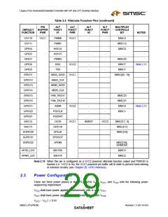
Table 2.4 Alternate Function Pins (continued)
PIN
BUFFER
PWR
ALT
FUNCT
#1
ALT
FUNCT
PWR
ALT
FUNCT
#2
ALT
FUNCT
PWR
MULTIPLEX
CONTROLS
BIT
DEFAULT
FUNCTION
NOTES
OUT10
OUT11
VCC1
PWM0
PWM1
VCC1
-
-
-
-
-
-
-
-
-
-
-
-
-
-
MISC4
MISC12
MISC9
GPIO4
KSO14
GPIO5
KSO15
GPIO7
PWM3
MISC22
MISC7
GPIO8
RXD
VCC2
VCC1
Note 2.15
GPIO9
TXD
MISC7
GPIO11
GPIO12
GPIO13
GPIO14
GPIO15
GPIO16
GPIO17
GPIO20
GPIO21
KSO12
KSO13
SGPIO30
SGPIO31
SGPIO32
AB2A_DATA
AB2A_CLK
AB2B_DATA
AB2B_CLK
FAN_TACH1
FAN_TACH2
A20M
MISC[20, 19]
MISC23
MISC21
MISC6
MISC1
VCC2
VCC1
-
-
Note 2.15
PS2CLK
PS2DAT
OUT8
-
-
-
-
VCC2
-
KBRST
-
MISC[17, 6]
MISC[17]
MISC[10]
GPIO18
SPCLK
SPDOUT
SPDIN
MISC[10],
SPIMODE
nFDD_LED
nPWR_LED
8051RX
8051TX
-
-
-
-
MISC3
MISC2
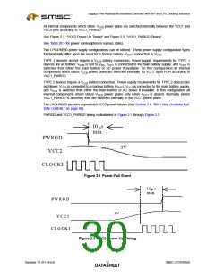
Note 2.15 When this pin is configured as a VCC2 powered alternate function output and PWRGD is
inactive (i.e. VCC2 is 0v), the VCC1 powered pin buffer will tri-state to prevent back-biasing
of external circuitry (see Chapter 20, GPIO Interface).
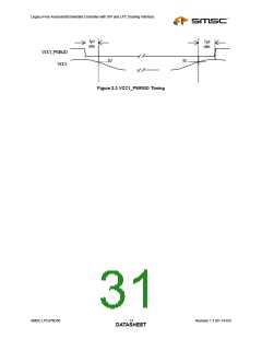
2.3
Power Configuration
There are three power planes in the LPC47N350 VCC0, VCC1, and VCC2 with the following power
sequencing requirement:
V
CC2 shall have power applied simultaneously with or after VCC1
.
.
VCC1 shall have power applied simultaneously with or after VCC0
VCC2 – VCC1 ≤ 0.5V
SMSC LPC47N350
11
Revision 1.1 (01-14-03)
DATASHEET

 SMSC [ SMSC CORPORATION ]