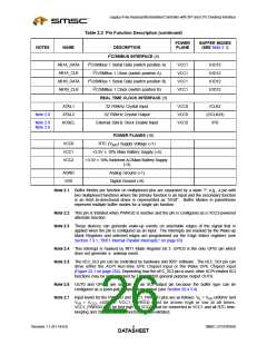
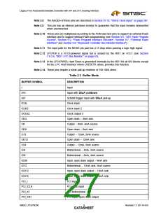
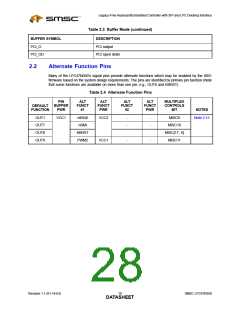
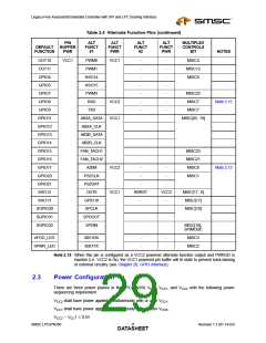
Legacy-Free Keyboard/Embedded Controller with SPI and LPC Docking Interface
All internal components which utilize VCC0 power plane are switched internally between the VCC1 and
VCC0 pins according to VCC1_PWRGD.
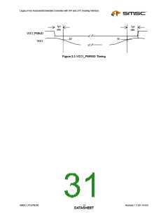
See Figure 2.2, "VCC2 Power-Up Timing" and Figure 2.3, "VCC1_PWRGD Timing".
See Table 28.3 for power consumption in various states.
Two LPC47N350 power supply configurations can be utilized. These power supply configuration types
fundamentally differ upon the need for a backup battery (VBAT) connection to VCC0
.
TYPE 1 devices do not require a VCC0 battery connection. Power supply requirements for TYPE 1
devices are as follows: VCC0 is tied to VSS, VCC1 is connected to the main battery supply, and VCC2 is
switched from either the main battery or AC power if available. In this configuration all internal
components which utilize VCC0 power plane are switched internally to VCC1 upon POR according to
VCC1_PWRGD.
TYPE 2 devices require a VCC0 battery connection. Power supply requirements for TYPE 2 devices are
as follows: VCC0 is connected to a backup battery (VBAT), VCC1 is connected to the main battery supply,
and VCC2 is switched from either the main battery or AC power if available. In this configuration all
internal components which utilize VCC0 power plane only when VCC1 is absent. Normally (when
VCC1_PWRGD is asserted) they are switched internally to the VCC1 power plane.
The LPC47N350 provides unpredicted VCC2 power failures (See Section 7.6, "8051 Ring Oscillator Fail-
Safe Controls," on page 46).
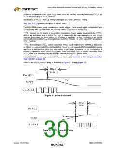
PWRGD and VCC1_PWRGD timing is illustrated in Figure 2.1 through Figure 2.3.
10 s
µ
min.
PWRGD
3V
VCC2
CLOCKI
Figure 2.1 Power-Fail Event
10 s
µ
m in.
P W R G D
3V
V C C 2
C L O C K I
Figure 2.2 VCC2 Power-Up Timing
Revision 1.1 (01-14-03)
SMSC LPC47N350
DATA1S2HEET

 SMSC [ SMSC CORPORATION ]