Legacy-Free Keyboard/Embedded Controller with SPI and LPC Docking Interface
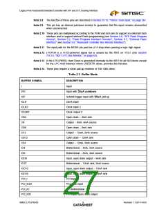
Table 2.3 Buffer Mode (continued)
DESCRIPTION
BUFFER SYMBOL
PCI_O
PCI output
PCI_OD
PCI open drain
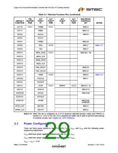
2.2
Alternate Function Pins
Many of the LPC47N350’s signal pins provide alternate functions which may be enabled by the 8051
firmware based on the system design requirements. The pins are identified by primary pin function (Note
that some functions are available on more than one pin; e.g., OUT8 and KBRST).
Table 2.4 Alternate Function Pins
PIN
BUFFER
PWR
ALT
FUNCT
#1
ALT
FUNCT
PWR
ALT
FUNCT
#2
ALT
FUNCT
PWR
MULTIPLEX
CONTROLS
BIT
DEFAULT
FUNCTION
NOTES
OUT1
OUT7
OUT8
OUT9
VCC1
nIRQ8
nSMI
VCC2
-
-
-
-
MISC0
MISC18
Note 2.15
KBRST
PWM2
MISC[17, 6]
MISC11
VCC1
-
-
Revision 1.1 (01-14-03)
SMSC LPC47N350
DATA1S0HEET

 SMSC [ SMSC CORPORATION ]