Legacy-Free Keyboard/Embedded Controller with SPI and LPC Docking Interface
Note 2.8 The function of these pins are described in Section 23.10, "32kHz Clock Input," on page 267.
Note 2.9 This pin has an internal pull-down resistor to guarantee that the input remains deasserted
when unconnected.
Note 2.10 These pins are multiplexed according to the PGM and nEA pins to support an external Flash
interface and to support internal Flash programming (see Section 9.6, "ATE Flash Program
Access", Section 9.2, "Flash Program Interface Decoder", Section 9.7, "External Flash
Interface" and Section 9.8, "Keyboard Controller Bus Monitor Interface").
Note 2.11 The input path for the MODE pin pad has a Vt drop when passing a logic high signal.
Note 2.12 LPCPD# is a VCC2-powered signal but is sensed by the 8051 on VCC1 (see Section
7.8.3.6, "8051 LPC Bus Monitor," on page 63).
Note 2.13 In the LPC47N350, Hard Reset is generated internally by the 8051 for all SIO blocks except
for the LPC Host Interface where LRESET#, alone, provides this function.
Note 2.14 These pins require a weak pull-up resistors of 10k-100k ohms.
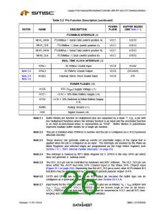
Table 2.3 Buffer Mode
BUFFER SYMBOL
DESCRIPTION
I
Input
IPD
Input with 30uA pulldown
Schmitt trigger input with 90uA pull-up
Clock input
ISP
ICLK
ICLK2
OCLK2
OD4
Clock input 2
Clock output 2
Open drain – 4mA sink
Output – 8mA, 4mA source
Open drain – 8mA sink
Output – 12mA, 6mA source
Open drain – 12mA sink
Output – 12mA, 6mA source
Bidirectional – 4mA, 2mA source
Bidirectional – 8mA, 4mA source
Input, open drain output – 8mA sink
Bidirectional – 12mA sink, 6mA source
Input, open drain output – 12mA sink
Input, open drain output – 16mA sink
PCI input
O8
OD8
O12
OD12
O24
IO4
IO8
IOD8
IO12
IOD12
IOD16
PCI_I
PCI_ICLK
PCI_IO
PCI_IOD
PCI clock input
PCI bidirectional
PCI input, open drain output
SMSC LPC47N350
9
Revision 1.1 (01-14-03)
DATASHEET

 SMSC [ SMSC CORPORATION ]