Legacy-Free Keyboard/Embedded Controller with SPI and LPC Docking Interface
The pins and descriptions in Table 2.2 are organized by primary pin function. For example, the PS2
Serial Clock and PS2 Serial Data pins are technically part of the KEYBOARD AND MOUSE INTERFACE
but are listed in the GENERAL PURPOSE I/O INTERFACE because the GPIO function of these pins is
the default.
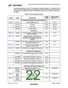
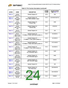
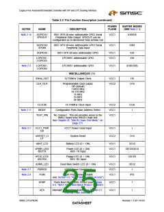
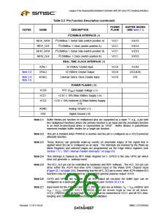
Table 2.2 Pin Function Description
POWER
PLANE
BUFFER MODES
NOTES
NAME
DESCRIPTION
(SEE Note 2.1)
PCI POWER MANAGEMENT AND SIRQ INTERFACE (4)
Note 2.5
nEC_SCI
PCI_CLK
SER_IRQ
CLKRUN#
Power Management Event
PCI Clock
VCC1
VCC2
VCC2
VCC2
PCI_OD
PCI_ICLK
PCI_IO
Serial IRQ
PCI Clock Control
LPC BUS (8)
PCI_OD
Note 2.14
Note 2.12
LAD[3:0]
LPCPD#
LPC address/data bus. Multiplexed command,
address and data bus.
VCC2
VCC1
PCI_IO
PCI_I
Powerdown Signal. Indicates that the
LPC47N350 should prepare for power to be
shut on the LPC interface. Used as LPC
powergood
LFRAME#
LRESET#
LDRQ[1]#
Frame signal. Indicates start of new cycle and
termination of broken cycle
VCC2
VCC2
VCC2
PCI_I
PCI_I
-
Note 2.13
Note 2.14
LPC Reset. LRESET# is the same as the
system PCI reset, PCIRST#
Encoded DMA request output for docking Super
I/O
DOCKING LPC INTERFACE (8)
DLAD[3:0]
LPC address/data bus for docking LPC Super
I/O
VCC2
-
DLFRAME#
DSER_IRQ
DCLKRUN#
DLDRQ[1]#
Frame signal for docking LPC Super I/O
Serial IRQ for docking LPC SUper I/O
VCC2
VCC2
VCC2
VCC2
-
-
-
-
PCI Clock Control for docking LPC Super I/O
Encoded DMA request output for docking Super
I/O
KEYBOARD AND MOUSE INTERFACE (28)
Note 2.10
KSO[0:11]/
ATE Prog.
Access/
Keyboard Scan Outputs (14 × 8).
NOTE: GPIO4 and GPIO5 can be configured as
KSO14 and KSO15 (16 × 8).
VCC1
OD4/IO4/IO4
Ext. Flash
Note 2.2
Note 2.3
KSO12
OUT8/
KBRST
Keyboard Scan Output
General Purpose Output
CPU_RESET
VCC1
VCC1
OD4/OD4/OD4
IOD4/IOD4
KSO13/
GPIO18
Keyboard Scan Output
General Purpose I/O
(WK_SE27)
Revision 1.1 (01-14-03)
4
SMSC LPC47N350
DATASHEET

 SMSC [ SMSC CORPORATION ]