Legacy-Free Keyboard/Embedded Controller with SPI and LPC Docking Interface
IFREN
XADR
XE
YE=SE=OE=MAS1=0
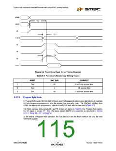
Trcv
Tnvh
ERASE
Tnvs
Terase
NVSTR
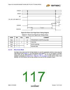
Figure 8.6 Flash Core Page Erase Timing Diagram
Table 8.11 Flash Core Page Erase Timing Values
NAME
MIN
MAX
UNITS
COMMENT
Tnvs
Terase
Tnvh
Trcv
5
2
5
1
µs
ms
µs
PROG/ERASE to NVSTR set up time
Erase time
4
NVSTR hold time
Recovery time
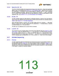
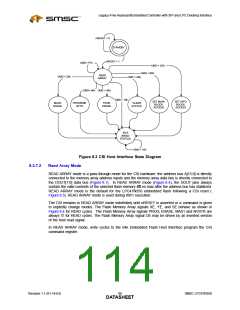
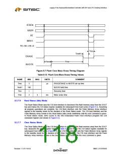
8.3.7.5
Mass Erase Mode
The Mass Erase mode uses the CSI flash interface to cycle the appropriate controls to mass erase the
Flash Memory Array (Figure 8.7). The Flash Memory Array signals YE, SE, OE, are always ‘0’ for Mass
Erase cycles; the XE signal behaves as shown in Figure 8.7. The CSI status register BUSY bit is
asserted as described in Section 8.3.6.1, "Busy Bit – D7," on page 94. At the end of a Mass Erase
operation, the host interface and the flash interface idle until the next command is given.
SMSC LPC47N350
Revision 1.1 (01-14-03)
DATA9S9HEET

 SMSC [ SMSC CORPORATION ]