Legacy-Free Keyboard/Embedded Controller with SPI and LPC Docking Interface
IFREN
Txa
XAD R
XE
Ty a
YADR
YE
SE
Toa
OE
DOUT
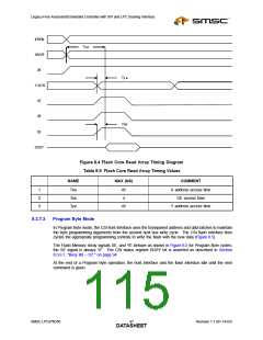
Figure 8.4 Flash Core Read Array Timing Diagram
Table 8.9 Flash Core Read Array Timing Values
MAX (NS)
NAME
COMMENT
1
2
3
Txa
Toa
Tya
45
4
X address access time
OE access time
45
Y address access time
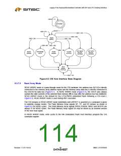
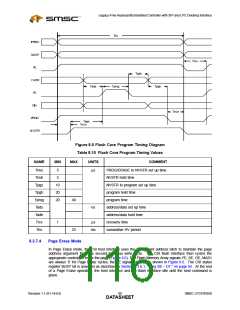
8.3.7.3
Program Byte Mode
In Program Byte mode, the CSI host interface uses the transparent address and data latches to maintain
the byte programming arguments from the second host bus write cycle. The CSI flash interface then
cycles the appropriate programming controls to write the flash with the new data (Figure 8.5).
The Flash Memory Array signals XE, and YE behave as shown in Figure 8.5 for Program Byte cycles;
the SE signal is always “0”. The CSI status register BUSY bit is asserted as described in Section
8.3.6.1, "Busy Bit – D7," on page 94.
At the end of a Program Byte operation, the host interface and the flash interface idle until the next
command is given.
SMSC LPC47N350
Revision 1.1 (01-14-03)
DATA9S7HEET

 SMSC [ SMSC CORPORATION ]