Legacy-Free Keyboard/Embedded Controller with SPI and LPC Docking Interface
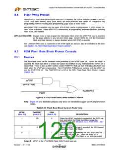
Note 8.9 FWRTPRT is the 8051 Flash Write Protect bit D0 in the Flash Boot Block Protect register
(Table 8.14).
Note 8.10 PGM is the LPC47N350 External Program Enable input pin.
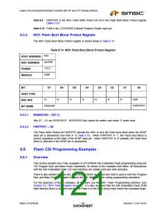
8.5.2
8051 Flash Boot Block Protect Register
The 8051 Flash Boot Block Protect register is shown below in Table 8.14.
Table 8.14 8051 Flash Boot Block Protect Register
N/A
HOST ADDRESS
8051 ADDRESS
POWER
0x7F88
VCC1
0x00
DEFAULT
BIT
D7
D6
D5
D4
D3
D2
D1
D0
-
-
-
-
-
-
-
-
HOST TYPE
8051 R/W
BIT NAME
R
R
R
R
R
R
R
R/W
Reserved
FWRTPRT
8.5.2.1
8.5.2.2
RESERVED – D[7:1]
Bits D7 – D1 are RESERVED. RESERVED bits cannot be written and return ‘0’ when read.
FWRTPRT – D0
The Flash Write Protect bit FWRTPRT permits the 8051 to lock the Flash boot block when the nFWP
input pin is deasserted (see item # in Table 8.13). When FWRTPRT is ‘1’, the Flash Boot Block is
locked, regardless of the state of the nFWP input pin. When FWRTPRT is ‘0’ (default), the Flash Boot
Block is unlocked if the nFWP pin is deasserted.
8.6
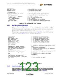
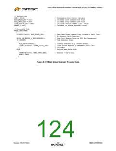
Flash CSI Programming Examples
8.6.1
Overview
This section provides two C-like examples of LPC47N350 64k Embedded Flash programming using the
CSI Program Byte and Mass Erase commands. As shown in the examples that follow, all transactions
with the 64k Embedded Flash CSI Host Interface are simple read and write functions.
There is also another function NO_ERRORS_&_BUSY described here that is used in both the Program
Byte and Mass Erase examples to check the CSI Status register during programming operations.
For the purposes of these examples all functions use the 8051 Flash Programming Interface (see
Section 9.4, "8051 Flash Program Access"). It is also assumed that the 64k Embedded Flash ROM
Main Memory Block is selected and that the Flash is in the Read Array mode before the examples begin.
SMSC LPC47N350
103
Revision 1.1 (01-14-03)
DATASHEET

 SMSC [ SMSC CORPORATION ]