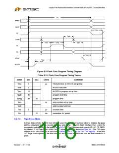
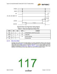
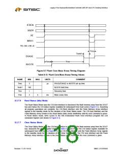
Legacy-Free Keyboard/Embedded Controller with SPI and LPC Docking Interface
8.4
Flash Write Protect
When the CSI Flash Write Protect input nWRTPRT is asserted, the bottom 2k bytes (0x0000 – 0x07FF)
of the Flash Main Memory Array (boot block) are write protected and cannot be changed by any
programming method including byte programming, page erase or mass erase.
When nWRTPRT is asserted only the upper 62k of flash can be re-programmed or page erased; i.e.,
mass erase is disabled. When nWRTPRT is deasserted, all programming and erase functions, including
mass erase, are enabled.
APPLICATION NOTE: To page erase or byte program the Information Block when the nWRTPRT input is asserted,
set the page address to any non-boot block page. MASS ERASE for both the Information
Block and Main Memory is always disabled when nWRTPRT is asserted.
The CSI nWRTPRT input is connected to the nFWP input pin and can also be controlled by the 8051
(see Section 8.5, "8051 Flash Boot Block Protect Controls").
8.5
8051 Flash Boot Block Protect Controls
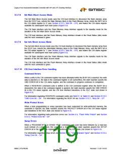
8.5.1
Overview
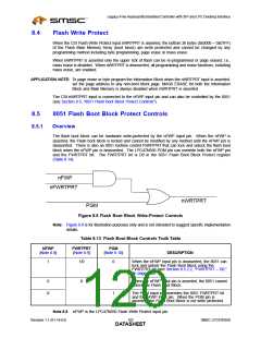
The flash boot block can be hardware write-protected by the nFWP input pin. When the nFWP is
asserted, the Flash boot block is locked and cannot be modified by any method until the nFWP pin is
deasserted. There is also an 8051 runtime control FWRTPRT that can lock and unlock the flash boot
block when the nFWP pin is deasserted. The LPC47N350 PGM pin can override both the nFWP pin
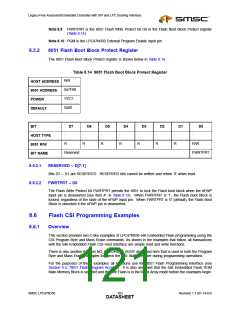
and the FWRTPRT bit. The FWRTPRT bit is D0 in the 8051 Flash Boot Block Protect register
(Table 8.14).
nFWP
nFWRTPRT
nWRTPRT
PGM
Figure 8.8 Flash Boot Block Write-Protect Controls
Note: Figure 8.8 is for illustration purposes only and is not intended to suggest specific implementation
details.
Table 8.13 Flash Boot Block Controls Truth Table
NFWP
FWRTPRT
PGM
(Note 8.8)
(Note 8.9)
(Note 8.10)
DESCRIPTION
1
1/0
0
When the nFWP input pin is deasserted, the 8051 can
lock and unlock the Flash Boot Block using the
FWRTPRT bit (see Section 8.5.2.2, "FWRTPRT – D0,"
on page 103).
0
X
When the nFWP input pin is asserted, the 8051 cannot
unlock the Flash Boot Block.
X
1
The PGM input pin overrides the 8051 FWRTPRT bit
and the nFWP input pin. When the PGM pin is
asserted, the Flash Boot Block is not write protected.
Note 8.8 nFWP is the LPC47N350 Flash Write Protect input pin.
Revision 1.1 (01-14-03)
102
SMSC LPC47N350
DATASHEET

 SMSC [ SMSC CORPORATION ]