SiI 1161 PanelLink Receiver
Data Sheet
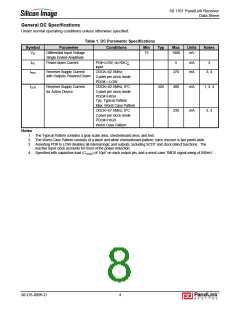
General DC Specifications
Under normal operating conditions unless otherwise specified.
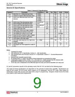
Table 1. DC Parametric Specifications
Symbol
Parameter
Differential Input Voltage
Single Ended Amplitude
Power-down Current
Conditions
Min
75
Typ
Max
1000
Units
mV
Notes
VID
IPD
PD#=LOW, no RXC+
input
5
mA
mA
3
IPDO
Receiver Supply Current
ODCK=82.5MHz,
270
3, 4
with Outputs Powered Down
2 pixel per clock mode
PDO# = LOW
ICCR
Receiver Supply Current
for Active Device
ODCK=82.5MHz, 0°C
2 pixel per clock mode
320
400
330
mA
mA
1, 2, 4
PDO#=HIGH
Typ: Typical Pattern
Max: Worst Case Pattern
ODCK=67.5MHz, 0°C
2 pixel per clock mode
PDO#=HIGH
2, 4
Worst Case Pattern
Notes
1. The Typical Pattern contains a gray scale area, checkerboard area, and text.
2. The Worst Case Pattern consists of a black and white checkerboard pattern; each checker is two pixels wide.
3. Asserting PD# to LOW disables all internal logic and outputs, including SCDT and clock detect functions. The
inactive input clock accounts for most of the power reduction.
4. Specified with capacitive load (CLOAD) of 10pF on each output pin, and a worst-case TMDS signal swing of 600mV.
SiI-DS-0096-D
4

 SILICONIMAGE [ Silicon image ]