SiI 1161 PanelLink Receiver
Data Sheet
Functional Description
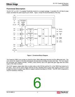
The SiI 1161 is a DVI 1.0 compliant PanelLink receiver in a compact package. It provides 24 or 48 bits for data
output, and allows for panel support up to UXGA. Figure 1 shows the functional blocks of the chip.
PIXS
HS_DJTR
OCK_INV
Control Registers
-----------
Termination
and
SCL
SDA
Equalization
Control
EXT_RES
RX2+
RX2-
Data Recovery
CH2
QE[23:0]
QO[23:0]
VCR
VCR
VCR
SYNC2
SYNC1
SYNC0
RX1+
RX1-
Data Recovery
CH1
ODCK
DE
Panel
Interface
Logic
Channel
SYNC
Decoder
HSYNC
VSYNC
RX0+
RX0-
Data Recovery
CH0
SCDT
CTL[3:1]
RXC+
RXC-
VCR
PLL
PDO#
STAG_OUT#
ST
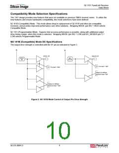
Figure 1. Functional Block Diagram
The PanelLink TMDS core accepts as inputs the three TMDS differential data lines and the differential clock. The
core senses the signals on the link and properly decodes them providing accurate pixel data. The core outputs
the necessary sync signals (HSYNC, VSYNC), clock (ODCK), and a DE signal that goes high when the active
region of the video is present.
The SCDT signal is output when there is active video on the DVI link and the PLL in the TMDS has locked on to
the video. SCDT can be used to trigger external circuitry, indicating that an active video signal is present or used
to place the device in power down when no signal is present (by tying it to PDO#). The EXT_RES component is
used for impedance matching.
SiI-DS-0096-D
2

 SILICONIMAGE [ Silicon image ]