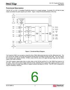
SiI 1161 PanelLink Receiver
Data Sheet
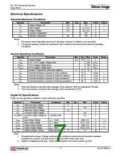
Electrical Specifications
Absolute Maximum Conditions
Symbol
VCC
VI
Parameter
Supply Voltage 3.3V
Input Voltage
Min
-0.3
-0.3
-0.3
Typ
Max
4.0
Units
V
Notes
1
VCC+ 0.3
VCC+ 0.3
125
V
VO
Output Voltage
V
2
TJ
Junction Temperature
Storage Temperature
°C
°C
TSTG
-65
150
Notes
1. Permanent device damage may occur if absolute maximum conditions are exceeded.
2. Functional operation should be restricted to the conditions described under Normal Operating
Conditions.
Normal Operating Conditions
Symbol
VCC
Parameter
Min Typ Max Units
Notes
Supply Voltage
3.0
3.3
3.6
200
100
75
V
VCCN
VCC, OVCC Supply Voltage Noise
mVP-P
mVP-P
mVP-P
°C
AVCCN
PVCCN
TA
AVCC Supply Voltage Noise
PVCC Supply Voltage Noise
Ambient Temperature (with power applied)
Thermal Resistance (Junction to Case) soldered
Thermal Resistance (Junction to Ambient) soldered
Thermal Resistance (Junction to Case) unsoldered
Thermal Resistance (Junction to Ambient) unsoldered
0
25
13
26
19
58
70
1
1
2
2
θJCS
θJAS
θJCU
θJAU
°C/W
°C/W
°C/W
°C/W
Notes
1. Thermal resistance specified with package ePad soldered 100% to underlying PCB pad.
2. Thermal resistance specified with package ePad unsoldered to PCB.
Digital I/O Specifications
Under normal operating conditions unless otherwise specified.
Symbol
VIH
Parameter
Conditions
Min
2
Typ
Max
Units
Notes
High-level Input Voltage
Low-level Input Voltage
High-level Output Voltage
Low-level Output Voltage
V
V
V
V
V
VIL
0.8
VOH
2.4
VOL
0.4
0.4
VOL(SDA) Low-level Output Voltage on
SDA
IOL(SDA)=3mA
VCINL
VCIPL
VCONL
VCOPL
IOL
Input Clamp Voltage
Input Clamp Voltage
Output Clamp Voltage
Output Clamp Voltage
Output Leakage Current
ICL = -18mA
ICL = 18mA
GND -0.8
IVCC + 0.8
GND -0.8
OVCC + 0.8
10
V
V
1, 2
1, 2
1
ICL = -18mA
ICL = 18mA
V
V
1
High Impedance
-10
µA
Note
1. Guaranteed by design. Voltage undershoot or overshoot cannot exceed absolute maximum
conditions for a pulse of greater than 3 ns or one third of the clock cycle.
2. Applies to toggling inputs only. Strap selected options are fixed at power-up time.
3
SiI-DS-0096-D

 SILICONIMAGE [ Silicon image ]