SiI 1161 PanelLink Receiver
Data Sheet
LIST OF TABLES
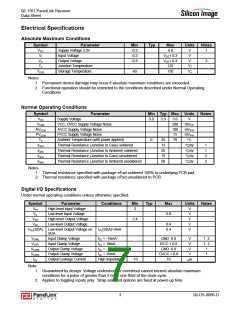
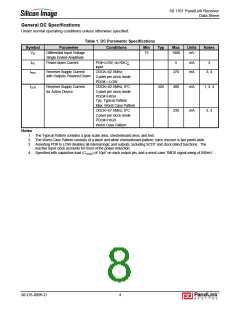
Table 1. DC Parametric Specifications ........................................................................................................... 4
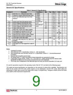
Table 2. General AC Specifications ................................................................................................................ 5
Table 3. SiI 161B Mode DC Specifications..................................................................................................... 7
Table 4. SiI 161B Mode AC Specifications ..................................................................................................... 8
Table 5. SiI 1161 Mode DC Specifications.................................................................................................... 10
Table 6. SiI 1161 Mode AC Specifications.................................................................................................... 11
Table 7. Sample Calculation of Data Output Setup and Hold Times – OCK_INV=0.................................... 13
Table 8. Sample Calculation of Data Output Setup and Hold Times – OCK_INV=1.................................... 14
Table 9. One Pixel per Clock Mode Data Mapping....................................................................................... 24
Table 10. Two Pixel per Clock Mode Data Mapping..................................................................................... 24
Table 11. One Pixel per Clock Input/Output TFT Mode – VESA P&D and FPDI-2TM Compliant.................. 25
Table 12. Two Pixels per Clock Input/Output TFT Mode.............................................................................. 26
Table 13. 24-bit One Pixel per Clock Input with 24-bit Two Pixels per Clock Output TFT Mode ................. 27
Table 14. 18-bit One Pixel per Clock Input with 18-bit Two Pixels per Clock Output TFT Mode ................. 28
Table 15. Two Pixels per Clock Input with One Pixel per Clock Output TFT Mode ..................................... 29
Table 16. Output Clock Configuration by Typical TFT Panel Application ..................................................... 30
Table 17. New Pin Functions for SiI 1161 in Programmable Mode.............................................................. 31
Table 18. Internal I2C Registers.................................................................................................................... 33
Table 19: I2C Register Field Definitions........................................................................................................ 34
Table 20. Recommended Components for 1-2MHz Noise Suppression...................................................... 36
Table 21. Recommended Components for 100-200kHz Noise Suppression on PVCC .............................. 36
LIST OF FIGURES
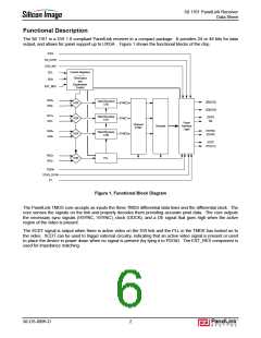
Figure 1. Functional Block Diagram ............................................................................................................... 2
Figure 2. SiI 161B Mode Control of Output Pin Drive Strength...................................................................... 6
Figure 3. Output Loading in SiI 161B Mode ................................................................................................... 9
Figure 4. SiI 1161 Mode Control of Output Pin Drive Strength....................................................................... 9
Figure 5. Receiver Output Setup and Hold Times – OCK_INV=0................................................................ 12
Figure 6. Receiver Output Setup and Hold Times – OCK_INV=1................................................................ 13
Figure 7. Digital Output Transition Times ..................................................................................................... 15
Figure 8. Receiver Clock Cycle/High/Low Times ......................................................................................... 15
Figure 9. Channel-to-Channel Skew Timing ................................................................................................ 15
Figure 10. Receiver Clock-to-Output Delay and Duty Cycle Limits ............................................................. 16
Figure 11. Output Signals Disabled Timing from Clock Inactive .................................................................. 16
Figure 12. Wake-Up on Clock Detect .......................................................................................................... 16
Figure 13. Output Signals Disabled Timing from PD# Active....................................................................... 17
Figure 14. SCDT Timing from DE Inactive or Active .................................................................................... 17
Figure 15. Two Pixels per Clock Staggered Output Timing Diagram........................................................... 17
Figure 16. I2C Data Valid Delay (driving Read Cycle data).......................................................................... 18
Figure 17. I2C Reset Timing at Power-Up or Prior to first I2C Acess............................................................ 18
Figure 18. Block Diagram for OCK_INV....................................................................................................... 22
Figure 19. I2C Byte Read.............................................................................................................................. 23
Figure 20. I2C Byte Write.............................................................................................................................. 23
Figure 21. RESET Generation Delay ........................................................................................................... 31
Figure 22. Recommended RESET Circuit.................................................................................................... 32
Figure 23. Voltage Regulation using TL431 ................................................................................................. 34
Figure 24. Voltage Regulation using LM317 ................................................................................................ 35
Figure 25. Decoupling and Bypass Capacitor Placement............................................................................ 35
Figure 26. Decoupling and Bypass Schematic............................................................................................. 36
Figure 27. Receiver Output Series Damping Resistors ............................................................................... 36
Figure 28. General Signal Routing Recommendations................................................................................ 37
Figure 29. Signal Trace Routing Example.................................................................................................... 37
Figure 30. ePad Diagram ............................................................................................................................. 39
Figure 31. Temperature Rise with Frequency and ePad.............................................................................. 40
Figure 32. Package Diagram........................................................................................................................ 41
SiI-DS-0096-D
iv

 SILICONIMAGE [ Silicon image ]