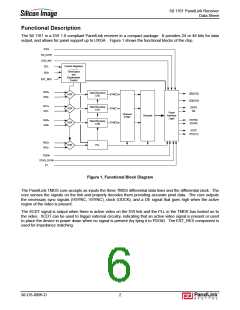
SiI 1161 PanelLink Receiver
Data Sheet
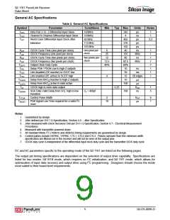
General AC Specifications
Table 2. General AC Specifications
Symbol
TDPS
Parameter
Conditions
165MHz
Min
Typ Max
245
4
Units
ps
Notes
Intra-Pair (+ to -) Differential Input Skew
Channel to Channel Differential Input Skew
Worst Case Differential Input Clock Jitter
tolerance
1
1
TCCS
165MHz
ns
TIJIT
65 MHz
465
270
182
40
ps
2,3
112 MHz
165 MHz
ps
ps
RCIP
FCIP
ODCK Cycle Time (one pixel per clock)
ODCK Frequency (one pixel per clock)
ODCK Cycle Time (two pixels per clock)
ODCK Frequency (two pixels per clock)
Output Clock Duty Cycle
one pixel per
clock
6
ns
1
1
1
1
7
1
1
1
25
165
80
MHz
ns
RCIP
two pixels per
clock
12
FCIP
12.5
40%
82.5
60%
10
MHz
TDUTY
TPDL
Delay PD# / PDO# Low to high-Z outputs
Link disabled (DE inactive) to SCDT low
Link enabled (DE active) to SCDT high
Delay from RXC+ Inactive to high-Z outputs
Delay from RXC+ active to data active
ODCK high to even data output
ns
ms
THSC
TFSC
50
4
10
DEedges
µs
TCLKPD
TCLKPU
TST
10
100
0.25
700
µs
RCIP
ns
1
5
SDA Data Valid Delay from SCL high to low
transition
CL = 400pf
TI2CDVD
TCTLW
Control Pulse Width
PD# Signal Low Time required for a valid I2C
reset
2
RCIP
6
1
TRESET
10
µs
Notes
1. Guaranteed by design.
2. Jitter defined per DVI 1.0 Specification, Section 4.6 – Jitter Specification.
3. Jitter measured with Clock Recovery Unit per DVI 1.0 Specification, Section 4.7 – Electrical Measurement
Procedures.
4. Measured with transmitter powered down.
5. All Standard Mode I2C (100kHz and 400kHz) timing requirements are guaranteed by design.
6. Control pulses include HSYNC, VSYNC, CTL1, CTL2 and CTL3. Pulses narrower than this minimum width
specification are filtered out in the receiver and will not be seen at the output pins.
7. ODCK duty cycle is independent of the differential input clock duty cycle and the transmitter IDCK duty cycle.
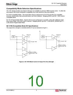
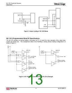
DC and AC parameters specific to the operating mode of the SiI 1161 are listed on the following pages.
The output pin timing specifications are dependent on the selection of output drive capability. Specifications are
listed for two modes: SiI 161B mode, which requires no I2C initialization; and SiI 1161 mode, which allows for
optimization of input data recovery and output drive using I2C programming. Designers should choose the mode
most suited to their board-level requirements.
5
SiI-DS-0096-D

 SILICONIMAGE [ Silicon image ]