SiI 1161 PanelLink Receiver
Data Sheet
SiI 161B (Compatible) Mode AC Specifications
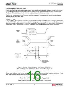
AC timings are provided here in setup/hold format at 165MHz for ease of direct comparison to the SiI 161B part.
Timing specifications in Table 4 apply to worst-case one pixel per clock mode. For other modes and frequencies
use the SiI 1161 Mode timings and calculation methodology, “Calculating Setup and Hold Times” on Page 12.
Table 4. SiI 161B Mode AC Specifications
Strap option: ST=0 (Low Drive Strength)
Parameter
Data, HSYNC, VSYNC
Conditions
Limits (ns)
Max
2.5
DHLT
DLHT
1-to-0 Transition
0-to-1 Transition
CL=5pF
CL=5pF
2.0
ODCK, DE
DHLT
Max
1.5
1-to-0 Transition
0-to-1 Transition
CL=5pF
CL=5pF
DLHT
1.7
Timing @ 165MHz
Min
Min
OCK_INV=0
OCK_INV=1
TSETUP
THOLD
Data
CL=5pF
CL=5pF
CL=5pF
CL=5pF
0.9
0.2
2.8
3.6
1.2
0.4
2.4
2.6
DE, HSYNC, VSYNC
Data
DE, HSYNC, VSYNC
Strap option: ST=1 (High Drive Strength)
Parameter
Conditions
Limits (ns)
Data, HSYNC, VSYNC
Max
2.5
DHLT
DLHT
1-to-0 Transition
0-to-1 Transition
CL=10pF
CL=10pF
2.0
ODCK, DE
DHLT
Max
1.2
1-to-0 Transition
0-to-1 Transition
CL=10pF
CL=10pF
DLHT
1.4
Timing @ 165MHz
Min
Min
OCK_INV=0
OCK_INV=1
TSETUP
THOLD
Data
CL=10pF
CL=10pF
CL=10pF
CL=10pF
0.9
0.6
2.8
3.1
1.2
1.1
2.2
2.1
DE, HSYNC, VSYNC
Data
DE, HSYNC, VSYNC
Notes
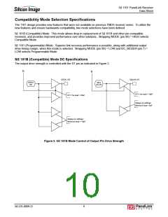
1. All transitions are specified at worst case of 70ºC with minimum VCC.
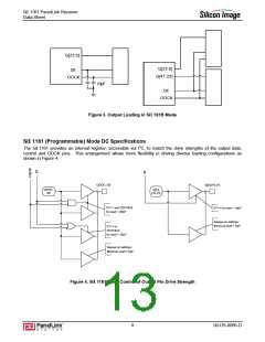
2. ODCK and DE output pins should be loaded with 10pF when ST=0 and 20pF when ST=1. If layout requires only a
point-to-point, one load net, a discrete 10pF capacitor should be added to the net to create these loads. See Figure
3.
SiI-DS-0096-D
8

 SILICONIMAGE [ Silicon image ]