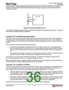
SiI 1161 PanelLink Receiver
Data Sheet
Decoupling and bypass capacitors are also involved with power supply connections, as described in detail in
Figure 26.
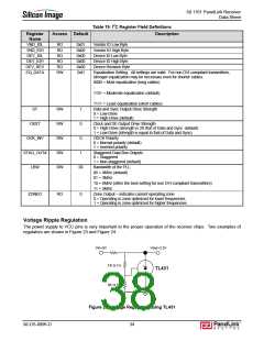
LM317EMP
Vin=5V
Vout=3.3V
Vin
Vout
ADJ
240 Ω 1%
390 Ω 1%
Figure 24. Voltage Regulation using LM317
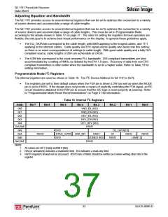
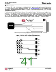
For the purposes of efficient power supply design, the relative power consumption of each of the power planes
can be estimated as follows as a percentage of total chip power consumption.
ꢁ
ꢁ
ꢁ
ꢁ
AVCC: 30-35%
DVCC: 30-40%
PVCC: 10-15%
OVCC: 20-40%
The power consumed by the OVCC power plane shows greater range than the others because of the variety of
loading possibilities. PVCC is the power plane that is most sensitive to excessive noise, but noise on this plane
can be controlled relatively easily due to the limited power consumed.
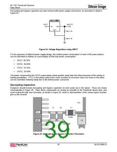
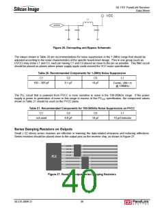
Decoupling Capacitors
Designers should include decoupling and bypass capacitors at each power pin in the layout. These are shown
schematically in Figure 26. Place these components as closely as possible to the PanelLink device pins, and
avoid routing through vias if possible, as shown in Figure 25, which is representative of the various types of power
pins on the receiver.
VCC
L1
C1
C2
VCC
GND
Ferrite
C3
Via to GND
Figure 25. Decoupling and Bypass Capacitor Placement
35
SiI-DS-0096-D

 SILICONIMAGE [ Silicon image ]