SiI 1161 PanelLink Receiver
Data Sheet
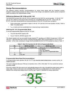
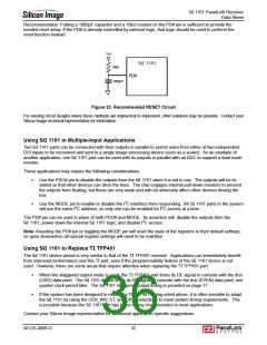
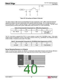
Recommendation: Putting a 1000pF capacitor and a 10kΩ resistor on the PD# pin is sufficient to provide the
needed reset delay. If the PD# is already controlled by external logic, that logic should be used to perform the
reset function instead.
Vcc
SiI 1161
10kΩ
PD#
1000pF
Figure 22. Recommended RESET Circuit
For existing circuit designs where these methods are impractical to implement, other solutions may be possible. Contact your
Silicon Image technical representative for information.
Using SiI 1161 in Multiple-Input Applications
Two SiI 1161 parts can be connected with their outputs in parallel to permit video from either of two independent
DVI inputs to be recovered and sent to a single image processing device (such as a scaler). As an example of
another application, one SiI 1161 part can be used with its outputs in parallel with an ADC to support a dual mode
monitor.
These applications may require the following considerations.
ꢁ
Use the PDO# pin to disable the outputs from the SiI 1161 when it is not in use. The outputs will be tri-
stated so that other devices can drive the lines. The chip engages internal pull-down resistors to prevent
the outputs from floating, but these are very weak and will not adversely affect other devices driving the
bus.
ꢁ
Use the MODE pin to enable or disable the I2C interface from responding. All SiI 1161 parts in the system
will use the same I2C address, so only one can be enabled for I2C access at a time.
The PD# pin can be used in place of both PDO# and MODE. Its assertion will: disable the outputs from the
SiI 1161; power down the internal SiI 1161 logic; and disable I2C access.
Note: Asserting the PD# pin or toggling the MODE pin will reset the state of the registers to their default settings,
so upon deassertion all special register settings will need to be rewritten.
Using SiI 1161 to Replace TI TFP401
The SiI 1161 device pinout is very similar to that of the TI TFP401 receiver. Applications can immediately benefit
from improved performance over the TI part, even if the programmability feature of the SiI 1161 device is not
used. However, there are some areas that require attention when replacing the TI TFP401 part.
ꢁ
When the staggered output mode is used, the TI TFP401 part times its DE signal to coincide with the first
(ODD) data pixel. The SiI 1161 device times its DE signal to coincide with the first (EVEN) data pixel, one
quarter clock period later. The SiI 1161 staggered output timing is provided on page.17.
ꢁ
If the system has been designed to match the TI TFP401 timing noted above, it is often possible to adapt
the SiI 1161 by using the OCK_INV, ST, and CKST selections to meet system timing requirements. This
is possible because the SiI 1161 part has better timing characteristics in most applications.
Contact your Silicon Image representative for additional application-specific suggestions.
SiI-DS-0096-D
32

 SILICONIMAGE [ Silicon image ]