SiI 1161 PanelLink Receiver
Data Sheet
Packaging
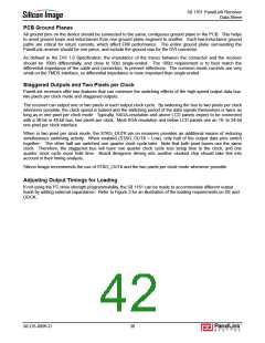
Thermal Design Options
The SiI 1161 is packaged in a thermally enhanced 100 pin TQFP with an exposed metal pad (6.5mmx 6.5mm) on
the package for improved thermal dissipation. With the worst-case power consumption and heat dissipation of
the SiI 1161, its exposed thermal pad requires soldering to the PCB. When operating below the maximum speed
of the SiI 1161, or in an environment with a maximum ambient lower than 70ºC, it may not be necessary to solder
the ePad to the PCB. The board designer should calculate the application-specific thermal resistance and
maximum resulting junction temperature.
Important: Do not place any vias or exposed signal traces beneath the exposed thermal metal pad of the
SiI 1161 on the PCB.
Additional specific guidelines for design of the thermal pad, the solder mask, etc. are on page 39.
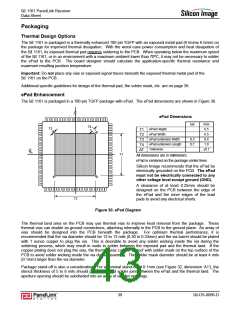
ePad Enhancement
The SiI 1161 is packaged in a 100-pin TQFP package with ePad. The ePad dimensions are shown in Figure 30.
C
ePad Dimensions
typ
max
6.5
T4
T3
ePad Height
T1
T2
T3
T4
∆T
ePad Width
6.5
ePad extension Width
ePad extension Length
Tolerance
0.3
0.7
0.4
1.0
±0.1
C
T1
All dimensions are in millimeters.
ePad is centered on the package center lines.
Silicon Image recommends that the ePad be
electrically grounded on the PCB. The ePad
must not be electrically connected to any
other voltage level except ground (GND).
A clearance of at least 0.25mm should be
designed on the PCB between the edge of
the ePad and the inner edges of the lead
pads to avoid any electrical shorts.
T2
Figure 30. ePad Diagram
The thermal land area on the PCB may use thermal vias to improve heat removal from the package. These
thermal vias can double as ground connections, attaching internally in the PCB to the ground plane. An array of
vias should be designed into the PCB beneath the package. For optimum thermal performance, it is
recommended that the via diameter should be 12 to 13 mils (0.30 to 0.33mm) and the via barrel should be plated
with 1 ounce copper to plug the via. This is desirable to avoid any solder wicking inside the via during the
soldering process, which may result in voids in solder between the exposed pad and the thermal land. If the
copper plating does not plug the vias, the thermal vias can be ‘tented’ with solder mask on the top surface of the
PCB to avoid solder wicking inside the via during assembly. The solder mask diameter should be at least 4 mils
(0.1mm) larger than the via diameter.
Package stand-off is also a consideration. For a nominal stand-off of 0.1mm (see Figure 32, dimension ‘A1’), the
stencil thickness of 5 to 8 mils should provide a good solder joint between the ePad and the thermal land. The
aperture opening should be subdivided into an array of smaller openings.
39
SiI-DS-0096-D

 SILICONIMAGE [ Silicon image ]