SiI 1161 PanelLink Receiver
Data Sheet
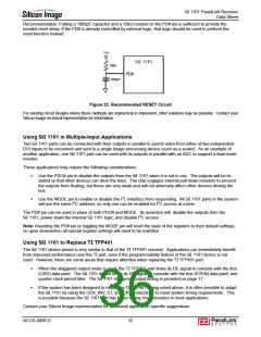
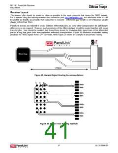
Adjusting Equalizer and Bandwidth
The SiI 1161 provides access to several internal registers that can be set to optimize the connection to a variety
of source devices and accommodate a range of cable lengths.
The SiI 1161 provides access to several internal registers that can be set to optimize the connection to a variety
of source devices and accommodate a range of cable lengths. Pins must be set in Programmable Mode
according to the details shown in Table 17 on page 31. The rules for setting the registers for best operation are
flexible; the only goal is to achieve best visual performance on the display. In general these guidelines apply.
ꢁ
The EQ_DATA bits correspond to the cable length, with 0000 applying to the longest cables, and 1111
applying to the shortest cables. Cable quality and DVI signal source quality also factor into this setting,
so there is no exact correspondence of settings to cable length. With good cable quality and a fully DVI-
compliant source, cable lengths of 20m are achievable at UXGA.
ꢁ
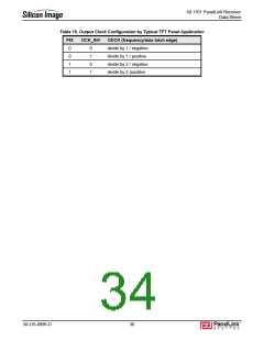
The LBW bits correspond to the clock recovery PLL bandwidth. DVI-compliant transmitters are best
accommodated by a setting of 4MHz as dictated by the DVI 1.0 spec. Recovery of data from non DVI-
compliant transmitters is often better when the bandwidth is set to a higher value. Refer to Table 19 for
setting information.
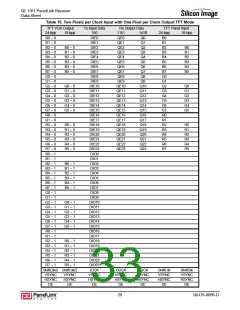
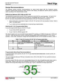
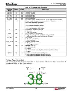
Programmable Mode I2C Registers
The internal registers are used as shown in Table 18. The I2C Device Address for SiI 1161 is 0x76.
•
The registers are set to their default values when the PD# pin is driven LOW (as well as when the MODE
pin is set to HIGH). If the design does not provide a means of explicitly controlling the PD# signal, an RC
circuit should be attached to the PD# pin to ensure that the I2C logic is reset properly at powerup. Refer
to “Programmable Mode Reset Recommendations” on Page 31 for information.
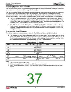
Table 18. Internal I2C Registers
Addr.
0x0
Bit 7
Bit 6
Bit 5
Bit 4
Bit 3
Bit 2
Bit 1
Bit 0
VND_IDL (RO)
0x1
VND_IDH (RO)
DEV_IDL (RO)
DEV_IDH (RO)
DEV_REV (RO)
RSVD
0x2
0x3
0x4
0x5-0x8
0x9
RSVD
STAG_OUT#
RSVD
EQ_DATA[3:0]
0xA
RSVD
OCK_INV
CKST
ST
RSVD
RSVD
0xB
ZONEO (RO)
RSVD
LBW[1:0]
0xC-0xF
Notes
RSVD
1. All values are Bit 7 [msb] and Bit 0 [lsb].
2. RW (or unmarked) indicates a read/write field. RO indicates a read-only field.
3. RSVD registers should not be accessed. RSVD bits or fields should be written as 0 when writing other bits in the
register.
33
SiI-DS-0096-D

 SILICONIMAGE [ Silicon image ]