SiI 1161 PanelLink Receiver
Data Sheet
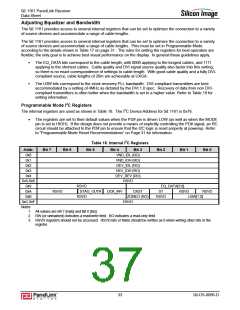
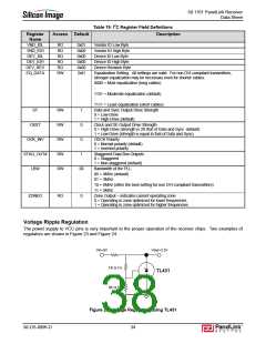
Table 19: I2C Register Field Definitions
Description
Register
Name
Access Default
VND_IDL
VND_IDH
DEV_IDL
DEV_IDH
DEV_REV
EQ_DATA
RO
RO
RO
RO
RO
RW
0x01
0x00
0x00
0x00
0x00
0xD
Vendor ID Low Byte
Vendor ID High Byte
Device ID Low Byte
Device ID High Byte
Device Revision Byte
Equalization Setting. All settings are valid. For non DVI-compliant transmitters,
stronger equalization may be necessary even for shorter cables.
0000 = Most equalization (long cables)
:
1101 = Moderate equalization (default)
:
1111 = Least equalization (short cables)
ST
CKST
RW
RW
RW
RW
RW
1
0
Data and Sync Output Drive Strength
0 = Low-Drive
1 = High-Drive (default)
Clock and DE Output Drive Strength
0 = High-Drive (strength is 2X that of Data and Sync -default)
1 = Low-Drive (strength is equal to that of Data and Sync)
OCK_INV
STAG_OUT#
LBW
0
ODCK Polarity
0 = Normal polarity (default)
1 = Inverted polarity
1
Staggered Data Bus Outputs
0 = Staggered
1 = Non-staggered (default)
00
Bandwidth of the PLL:
00 = 4MHz (default)
01 = 3MHz
10 = 6MHz (often the best setting for non DVI-compliant transmitters)
11 = 5MHz
ZONEO
RO
0
Zone Output – indicates current operating zone
0 = Operating in zone optimized for lower frequencies
1 = Operating in zone optimized for higher frequencies
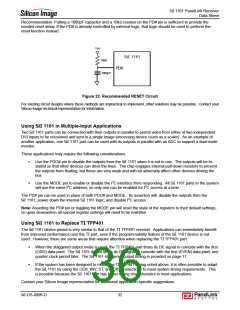
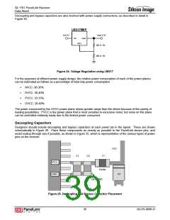
Voltage Ripple Regulation
The power supply to VCC pins is very important to the proper operation of the receiver chips. Two examples of
regulators are shown in Figure 23 and Figure 24.
Vin=5V
Vout=3.3V
1K Ω 1%
3K Ω 1%
TL431
Figure 23. Voltage Regulation using TL431
SiI-DS-0096-D
34

 SILICONIMAGE [ Silicon image ]