SiI 1161 PanelLink Receiver
Data Sheet
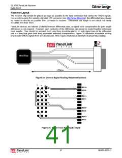
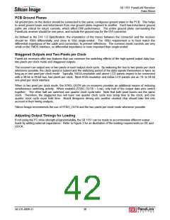
PCB Ground Planes
All ground pins on the device should be connected to the same, contiguous ground plane in the PCB. This helps
to avoid ground loops and inductances from one ground plane segment to another. Such low-inductance ground
paths are critical for return currents, which affect EMI performance. The entire ground plane surrounding the
PanelLink receiver should be one piece, and include the ground vias for the DVI connector.
As defined in the DVI 1.0 Specification, the impedance of the traces between the connector and the receiver
should be 100Ω differentially, and close to 50Ω single-ended. The 100Ω requirement is to best match the
differential impedance of the cable and connectors, to prevent reflections. The common mode currents are very
small on the TMDS interface, so differential impedance is more important than single-ended.
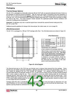
Staggered Outputs and Two Pixels per Clock
PanelLink receivers offer two features that can minimize the switching effects of the high-speed output data bus:
two pixels per clock mode and staggered outputs.
The receiver can output one or two pixels in each output clock cycle. By widening the bus to two pixels per clock
whenever possible, the clock speed is halved and the switching period of the data signals themselves is twice as
long as in one pixel per clock mode. Typically, SXGA-resolution and above LCD panels expect to be connected
with a 36-bit or 48-bit bus, two pixels per clock. Most XGA-resolution and below LCD panels use an 18- to 24-bit
one pixel per clock interface.
When in two pixel per clock mode, the STAG_OUT# pin on receivers provides an additional means of reducing
simultaneous switching activity. When enabled (STAG_OUT# = Low), only half of the output data pins switch
together. The other half are switched one quarter clock cycle later. Note that both pixel buses use the same
clock. Therefore, the staggered bus will have one quarter clock cycle less setup time to the clock, and one
quarter clock cycle more hold time. Board designers driving into another clocked chip should take this into
account in their timing analysis.
Silicon Image recommends the use of STAG_OUT# and the two pixels per clock mode whenever possible.
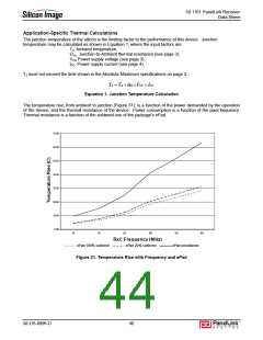
Adjusting Output Timings for Loading
If not using the I2C drive strength programmability, the SiI 1161 can be made to accommodate different output
loads by adding external capacitance. Refer to Figure 3 for an illustration of the loading requirements on DE and
ODCK.
SiI-DS-0096-D
38

 SILICONIMAGE [ Silicon image ]