LC7218, 7218M, 7218JM
Continued from preceding page.
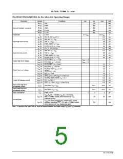
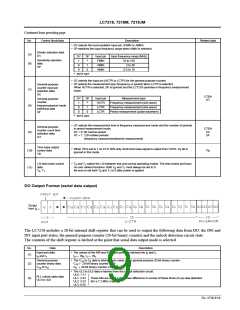
No.
Control block/data
Description
Related data
• DV selects the local oscillator input pin. (FMIN or AMIN)
• SP switches the input frequency range when AMIN is selected.
Divider selection data
DV
(5)
(6)
DV
1
SP
*
Input pin
FMIN
Input frequency range (MHz)
Sensitivity selection
data
SP
10 to 130
2 to 40
0
1
AMIN
0
0
AMIN
0.5 to 10
* don’t care
• SC selects the input pin (HCTR or LCTR) for the general-purpose counter.
• SF selects the measurement type (frequency or period) when LCTR is selected.
When HCTR is selected, SF is ignored and the LC7218 operates in frequency measurement
mode.
General-purpose
counter input pin
selection data
SC
(7)
(8)
CTEN
GT
DV
1
SP
*
Input pin
HCTR
LCTR
Measurement type
General-purpose
counter
frequency/period mode
switching data
SF
Frequency measurement (sine wave)
Frequency measurement (sine wave)
Period measurement (pulse waveform)
0
1
0
0
LCTR
* don’t care
• GT selects the measurement time in frequency measurement mode and the number of periods
in period measurement mode.
GT = 0: 60 ms/one period
General-purpose
counter count time
selection data
GT
CTEN
SC
SF
(9)
GT = 1: 120 ms/two periods
(frequency measurement/period measurement)
Time base output
control data
TB
• When TB is set to 1 an 8 Hz 40% duty clock time base signal is output from OUT0. O bit is
0
ignored in this mode.
O
0
(10)
(11)
LSI test mode control
data
• T and T switch the LSI between test and normal operating modes. The test modes and have
0
1
no user related functions. Both T and T must always be set to 0.
0 1
T , T
Be sure to set both T and T to 0 after power is applied.
0 1
0
1
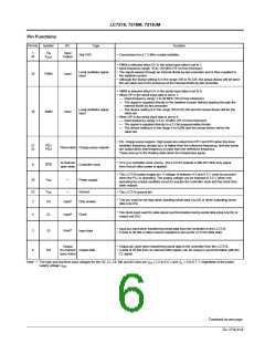
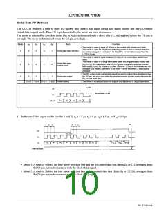
DO Output Format (serial data output)
The LC7218 includes a 28-bit internal shift register that can be used to output the following data from DO: the IN0 and
IN1 input port states, the general-purpose counter (20-bit binary counter) and the unlock detection circuit state.
The contents of the shift register is latched at the point that serial data output mode is selected.
No.
(1)
Data
Description
Input port data
• The values of the IN0 and IN1 input ports are latched into I and I .
0
1
I
and I
I ← IN , I ← IN
0 0 1 1
0
1
General-purpose
• The C to C data is latched from value of the general-purpose 20-bit binary counter.
19 0
(2)
(3)
counter binary data
C
← 20-bit binary counter MSB
19
C
to C
C → 20-bit binary counter LSB
0
19
0
• The UL3 to UL0 data is latched from the unlock detection circuit.
UL0: 1.11
UL1: 2.22
UL2: 3.33
UL3: 0.55
PLL unlock state data
UL3 to UL0
These bits are set to 1 if a phase difference in excess of these times (in µs) was detected.
(for a 7.2 MHz crystal)
No. 4758-9/16

 SANYO [ SANYO SEMICON DEVICE ]