LC7218, 7218M, 7218JM
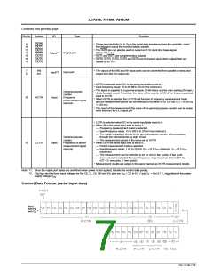
The LC7218 control data consists of 36 bits. All 36 bits must be input after power is applied to set up the LC7218 initial
state. This is because the last two bits, while being unrelated to user functions, are data that switches the LSI test modes.
Once the LC7218 has been initialized, the contents of the first 24 bits (D to CTEN) can be changed without changing
0
the contents of the last 12 bits (R0 to T1) by inputting data to DI in serial data input mode.
No.
Control block/data
Description
Related data
• This data sets up the programmable divider.
to D is a binary value with D as the MSB.
D
0
15
15
The position of the LSB is changed by DV and SP as listed in the table below.
DV
1
SP
*
LSB
D0
Divisor setting
256 to 65536
Actual divisor
Twice the set value
The set value
Programmable divider
data
DV
SP
(1)
D
to D
15
0
0
1
D0
256 to 65536
4 to 4096
0
0
D4
The set value
* don’t care
When D is the LSB, bits D to D are ignored.
4
0
3
• Data that determines the states of the output ports OUT0 to OUT6. O determines the
0
OUT0 pin output. However, note that when O is 0, OUT0 will output a high level, and when O
0
0
is 1, OUT0 will output a low level. O to O function in the same manner.
1
6
• These can be used for a wide range of purposes, including, for example, band switching
signals.
Output port data
to O
(2)
TB
O
0
6
• When the TB bit is set to 1, the O data is ignored and the OUT0 pin outputs an 8 Hz clock
0
time base signal.
• Since the output port states are undefined when power is first applied, transfer the control data
quickly.
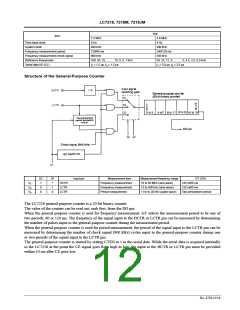
• Data that determines the operation of the general-purpose counter. When CTEN is 0, the 20-bit
binary counter (the general-purpose counter) is reset and the HCTR and LCTR pins are pulled
down to ground. When CTEN is set to 1, the general-purpose counter reset state is cleared and
the counter operates according to the SC bit (the general-purpose selection data). In this state,
the general-purpose counter will count either the HCTR or LCTR input signal.
General-purpose counter
initial data
CTEN
SC
SF
GT
(3)
• Since the general-purpose counter is reset by setting CTEN to 0, the result of a count operation
must be sent to the controller while CTEN is still 1.
• Data that selects one of the ten LC7218 reference frequencies or sets the LC7218 to
backup mode in which PLL operation is disabled.
R
R
R
R
3
Reference frequency (kHz)
0
1
2
0
0
0
0
100
50
0
0
0
0
0
0
0
1
1
1
1
1
1
1
1
0
0
0
1
1
1
1
0
0
0
0
1
1
1
1
0
1
1
0
0
1
1
0
0
1
1
0
0
1
1
1
0
1
0
1
0
1
0
1
0
1
0
1
0
1
25
25
12.5
6.25
3.125
3.125
10
Reference frequency
data
(4)
R
to R
3
0
9
5
1
PLL inhibit state*
Note: * PLL inhibit (backup mode)
The programmable divider block is turned off, both the FMIN and AMIN pins are pulled
down to ground, and the charge pump outputs go to the floating state.
Continued on next page.
No. 4758-8/16

 SANYO [ SANYO SEMICON DEVICE ]