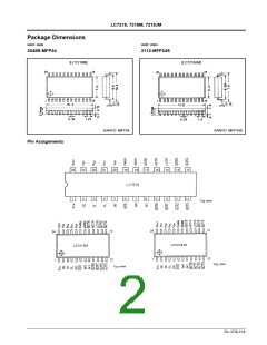
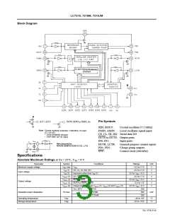
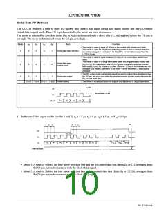
LC7218, 7218M, 7218JM
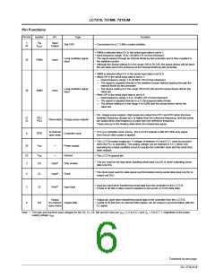
Pin Functions
Pin No. Symbol
I/O
Type
Function
X
1
24
Input
Output
IN
Xtal OSC
• Connections for a 7.2 MHz crystal oscillator
X
OUT
• FMIN is selected when DV in the serial input data is set to 1.
• Input frequency range: 10 to 130 MHz (70 mVrms minimum)
• The signal passes through an internal divide-by-two prescaler and is then supplied to
the swallow counter.
Local oscillator signal
input
19
FMIN
Input
• Although the divisor setting is in the range 256 to 65,536, the actual divisor will be twice
the set value due to the presence of the internal divide-by-two prescaler.
• AMIN is selected when DV in the serial input data is set to 0.
• When SP in the serial input data is set to 1:
— Input frequency range: 2 to 40 MHz (70 mVrms minimum).
— The signal is supplied directly to the swallow counter without passing through the
internal divide-by-two prescaler.
Local oscillator signal
input
— The divisor setting is in the range 256 to 65,536 and the actual divisor will be the
value set.
18
AMIN
Input
• When SP in the serial input data is set to 0:
— Input frequency range: 0.5 to 10 MHz (70 mVrms minimum).
— The signal is supplied directly to a 12-bit programmable divider.
— The divisor setting is in the range 4 to 4,096 and the actual divisor will be the
value set.
• PLL charge pump outputs. High levels are output from PD1 and PD2 when the local
oscillator frequency divided by n is higher than the reference frequency, and low levels
are output when that frequency is lower than the reference frequency.
These pins go to the floating state when the frequencies agree.
21
22
PD1
PD2
Three-state Charge pump outputs
N-channel
• SYC is a controller clock source. The LC7218 outputs a 400 kHz 66% duty signal
from this pin after power is applied.
6
SYC
Controller clock
open drain
• The LC7218 power supply pin. A voltage of between 4.5 and 6.5 V must be provided
when the PLL is operating. The supply voltage can be lowered to 3.5 V when only
operating the crystal oscillator circuit to acquire the controller clock and the clock time
base outputs.
V
20
—
Power supply
DD
V
23
2
—
Ground
• The LC7218 ground pin
SS
• This pin must be set high when inputting serial data (via DI) or when outputting serial
data (via DO).
CE
CL
Input*
Chip enable
• The clock input used for data signal synchronization during serial data input (via DI) or
output (via DO).
4
3
Input*
Input*
Output
Clock
• Input pin used when transferring serial data from the controller to the LC7218.
• A total of 36 bits of data must be supplied to set up the LC7218 initial state.
DI
Input data
• Output pin used when transferring serial data to the controller from the LC7218.
• A total of 28 bits from an internal shift register can be output in synchronization with the
CL signal.
5
DO
(N-channel Output data
open drain)
Note: * The high and low level input voltages for the CE, CL, DI, IN0 and IN1 pins are V = 2.2 to 6.5 V and V = 0 to 0.7 V, regardless of the power
IH
IL
supply voltage V
.
DD
Continued on next page.
No. 4758-6/16

 SANYO [ SANYO SEMICON DEVICE ]