OneNAND512Mb(KFG1216U2B-xIB6)
FLASH MEMORY
4.0 DC CHARACTERISTICS
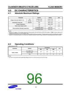
4.1
Absolute Maximum Ratings
Parameter
Symbol
Rating
-0.5 to + 4.6
-0.5 to + 4.6
-40 to +125
-65 to +150
5
Unit
Vcc
Vcc (for 3.3V)
VIN (for 3.3V)
Tbias
Voltage on any pin relative to VSS
V
All Pins
Industrial
Temperature Under Bias
Storage Temperature
°C
°C
Tstg
Short Circuit Output Current
IOS
mA
TA (Extended Temp.)
TA (Industrial Temp.)
-30 to +85
-40 to +85
Recommended Operating Temperature
°C
NOTES:
1. Minimum DC voltage is -0.5V on Input/ Output pins. During transitions, this level should not fall to POR level(typ. 1.8V@3.3V device). Maximum DC
voltage may overshoot to Vcc+2.0V for periods <20ns.
2. Permanent device damage may occur if ABSOLUTE MAXIMUM RATINGS are exceeded. Functional operation should be restricted to the conditions
detailed in the operational sections of this data sheet. Exposure to absolute maximum rating conditions for extended periods may affect reliability.
4.2
Operating Conditions
Voltage reference to GND
3.3V Device
Typ.
Parameter
Symbol
Unit
Min
2.7
0
Max
3.6
0
VCC-core / Vcc
VCC- IO / Vccq
VSS
3.3
0
V
V
Supply Voltage
NOTES:
1. Vcc-Core (or Vcc) should reach the operating voltage level prior to or at the same time as Vcc-IO (or Vccq).
96

 SAMSUNG [ SAMSUNG ]