OneNAND512Mb(KFG1216U2B-xIB6)
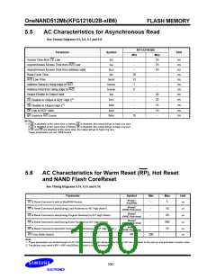
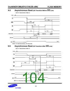
5.5 AC Characteristics for Asynchronous Read
FLASH MEMORY
See Timing Diagrams 6.5, 6.6, 6.7 and 6.8.
KFG1216U2B
Parameter
Symbol
Unit
Min
Max
76
76
76
-
Access Time from CE Low
tCE
tAA
-
-
ns
ns
ns
ns
ns
ns
ns
ns
ns
Asynchronous Access Time from AVD Low
Asynchronous Access Time from address valid
Read Cycle Time
tACC
tRC
-
76
12
7
6
-
AVD Low Time
tAVDP
tAAVDS
tAAVDH
tOE
-
Address Setup to rising edge of AVD
Address Hold from rising edge of AVD
Output Enable to Output Valid
-
-
20
20
CE Disable to Output & RDY High Z1)
tCEZ
tOEZ
-
OE Disable to Output High Z1)
CE Low to RDY Valid
-
-
15
15
-
ns
ns
ns
tCER
tWEA
WE Disable to AVD Enable
15
NOTE:
1. If OE is disabled at the same time or before CE is disabled, the output will go to high-z by tOEZ.
If CE is disabled at the same time or before OE is disabled, the output will go to high-z by tCEZ.
If CE and OE are disabled at the same time, the output will go to high-z by tOEZ.
These parameters are not 100% tested.
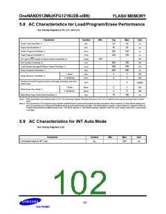
5.6
AC Characteristics for Warm Reset (RP), Hot Reset
and NAND Flash CoreReset
See Timing Diagrams 6.14, 6.15 and 6.16.
Parameter
Symbol
Min
Max
Unit
tReady1
(BootRAM)
RP & Reset Command Latch to BootRAM Access
µs
-
5
tReady2
(NAND Flash Array)
RP & Reset Command Latch(During Load Routines) to INT High (Note1)
RP & Reset Command Latch(During Program Routines) to INT High (Note1)
RP & Reset Command Latch(During Erase Routines) to INT High (Note1)
µs
µs
µs
-
-
-
10
20
tReady2
(NAND Flash Array)
tReady2
(NAND Flash Array)
500
tReady2
(NAND Flash Array)
RP & Reset Command Latch(NOT During Internal Routines) to INT High (Note1)
RP Pulse Width (Note2)
µs
-
10
-
tRP
ns
200
Note:
1. These parameters are tested based on INT bit of interrupt register. Because the time on INT pin is related to the pull-up and pull-down resistor value.
2. The device may reset if tRP < tRP min(200ns), but this is not guaranteed.
100

 SAMSUNG [ SAMSUNG ]