OneNAND512Mb(KFG1216U2B-xIB6)
FLASH MEMORY
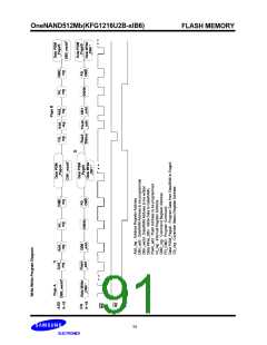
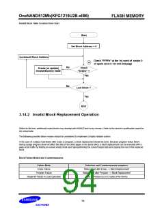
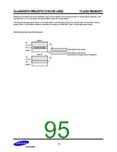
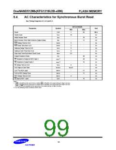
Referring to the diagram for further illustration, when an error happens in the nth page of block 'A' during program operation, copy
the data in the 1st ~ (n-1)th page to the same location of block 'B' via data buffer0.
Then copy the nth page data of block 'A' in the data buffer1 to the nth page of block 'B' or any free block. Do not further erase or
program block 'A' but instead complete the operation by creating an 'Invalid Block Table' or other appropriate scheme.
Block Replacement Operation Sequence
Block A
1st
1
{
(n-1)th
nth
an error occurs.
Data Buffer0 of the device
(page)
1
Data Buffer1 of the device
Block B
(assuming the nth page data is maintained)
1st
2
{
(n-1)th
nth
(page)
95

 SAMSUNG [ SAMSUNG ]