OneNAND512Mb(KFG1216U2B-xIB6)
FLASH MEMORY
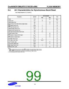
5.4
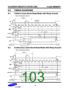
AC Characteristics for Synchronous Burst Read
See Timing Diagrams 6.1, 6.2 and 6.3.
Parameter
KFG1216U2B
Symbol
Unit
Min
1
Max
66
-
Clock
CLK
tCLK
tIAA
MHz
ns
ns
ns
ns
ns
ns
ns
ns
ns
ns
Clock Cycle
15
-
Initial Access Time
70
11
-
Burst Access Time Valid Clock to Output Delay
AVD Setup Time to CLK
tBA
-
tAVDS
tAVDH
tACS
tACH
tBDH
tOE
5
AVD Hold Time from CLK
2
-
Address Setup Time to CLK
Address Hold Time from CLK
Data Hold Time from Next Clock Cycle
Output Enable to Data
5
-
6
-
2.5
-
-
20
20
1)
CE Disable to Output & RDY High Z
-
tCEZ
1)
OE Disable to Output High Z
CE Setup Time to CLK
CLK High or Low Time
-
15
-
ns
ns
ns
ns
ns
ns
ns
tOEZ
tCES
6
tCLKH/L
tCLK/3
-
CLK 2) to RDY valid
tRDYO
-
-
11
11
-
CLK to RDY Setup Time
RDY Setup Time to CLK
CE low to RDY valid
tRDYA
tRDYS
tCER
4
-
15
Note
1. If OE is disabled at the same time or before CE is disabled, the output will go to high-z by tOEZ.
If CE is disabled at the same time or before OE is disabled, the output will go to high-z by tCEZ.
If CE and OE are disabled at the same time, the output will go to high-z by tOEZ.
2. It is the following clock of address fetch clock.
99

 SAMSUNG [ SAMSUNG ]